Go Back to GBS
Tags: console computer arcade video mod
There are a lot of people buying fancy upscalers these days. And who can blame them? Old videogames are great, but new monitors are lazy and inept. What, the signal is too slow for you? Clearly all these great old arcade boards, computers, and game consoles are just not a big enough challenge for the input logic in modern LCDs, who prefer to spend their considerable brainpower decoding much higher-frequency syncs. To solve this problem, I’ll spend not very much money.
What is a GBS board?
First, in case you’re not familiar, there is a family of loosely-aligned upscalers based around the Trueview 5725 chipset. Colloquially, they’re referred to as “GBS” boards, because of the two most popular models: GBS-8200 and GBS-8220. Being that it originates from the Chinese market, there is a confusing mix of different vendors slapping their own unique names and configurations on the product.
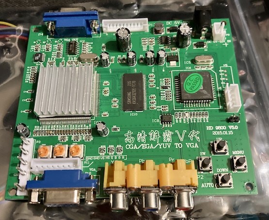
These upscaler boards are sold in China predominantly for – I’m guessing – using modern LCDs as legacy 15kHz arcade monitors, but have become popular on the Western internet for all kinds of 15kHz RGB systems. I first became aware of them when Ian Stedman was doing all of his experiments with fixing the video noise inherent to the board design, and bought one with the intent of eventually using it on my Atari 1040ST.
Of course, once the upscaler arrived, I tried it once or twice, couldn’t get it to work, and put it back in the box. Now it’s time for some revenge. And by revenge, I mean I’m going to cut its brains out and put new brains in.
What is GBS-Control?
The GBS-Control firmware lets an ESP8266-based microcontroller hijack the upscaler. Normally, the upscaler chipset is driven by an onboard microcontroller, but the firmware for that microcontroller absolutely stinks.
That’s why a bunch of hobbyists spent hundreds of hours figuring out how to control the GBS, and it turns out that the chipset is actually very versatile and produces great results. And since the ESP8266 microcontroller is most famous for inexpensive wi-fi, the project also features a web server frontend from which you can tweak all the options.
My hope with this project was that adding a cheapo ESP8266 evaluation board ($4) to my cheapo GBS board ($20) would produce a cheapo 15kHz RGB upscaler setup for a supergun or miscellaneous weirdo computer. And hey, I already have the parts on hand!
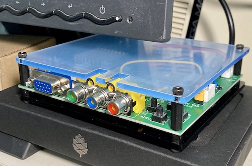
Last summer, expecting that I would soon have to build this project, I ordered an acrylic case for the GBS from Chipnetics. It turns out that the guy running that store is actually in the next city over, so I had a friend pick it up for me in order to save the handful of bucks that Canada Post would have wanted. The case is really nice, and makes me wonder if something similar could be done for the Leako.
Preparing the ESP8266
It may not surprise you to hear that I have a little bit of a bad habit of collecting el-cheapo development boards before I have a project in mind. I ended up using one of these “D1 mini” boards, which seem to be available from a thousand different vendors under their own names. In this case, the vendor’s name is “KeeYees,” which sounds like a fun place to work if only because you get to say the name a lot.
After installing all the libraries and checking out the master tarball of the gbs-control source, it built quickly and flashed itself onto the dev board. I was able to navigate to it on my phone via wifi, and tell it how to join my wireless LAN – very slick. Now for the rest of the job.
Attaching the ESP8266
This actually took me a surprisingly long time, and it’s all because of one little ground pin. There’s a four-pin header alongside the microcontroller IC that breaks out SCL/SDA serial, 3.3V and ground, and the install instructions tell you to use those pins.
Of course, the “ground” pin is connected to the beefiest ground plane I think I’ve ever tried to desolder. It took me a lot of time, flux, and the boost-mode on the Pinecil just to get the solder to flow at all. A desoldering needle finished the job. If I had to do it again, I would probably pre-heat the board with a hotplate first. When it was done, the entire board was too hot to the touch to comfortably pick up.
The worst part is that I didn’t even need to desolder that ground pin – all I needed from this connector was the SCL and SDA pins. I ended up using a small JST harness that came in the bag with the GBS to power the ESP8266 board through its pre-regulator 5V pin.
Out of all the things I’m not proud of on this project, I’m least proud of the wiring job I did here. Because I was in a rush, everything was done with the stranded 22AWG wire I had on the bench, and it looks extremely sloppy. I’d like to redo this at some point in the future, but I needed this quickly for another project, and only had about an hour to build this whole thing.
Excuses, excuses…
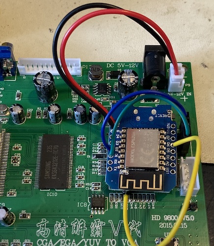
Because it seemed like SCL and SDA were likely to be reversed by accident, I crimped them for a Dupont-style connector and then put in a junk-drawer 0.1” pin header so I could swap them at test time if I had screwed up. Of course, this meant that the female connector shroud would be too tall for the case to close when it was all installed – I didn’t learn my lesson from the Famicom mod about how long these damn things are.
However, I left plenty of room to cut off the end, strip the wires, and solder them down permanently once I got the configuration right.
Now to test.
Test Run
Getting a power adapter was fairly easy – I had a variety of centre-positive 5V power bricks which had come with other gadgets from China, and used one that came from a faintly disappointing RF-to-AV converter. Of course, I did a quick continuity check first, as the barrel polarity did not seem to be listed anywhere on the GBS board.
I plugged this contraption into the PC-8801MH and fired it up. In order to get all those boogying electrons in the right place, I used a tangle of cables: Japanese 15-pin RGB-to-VGA, to a male-male SVGA extension cable, to the GBS, to the NEC 1970NX that I already know displayed the 24kHz from the PC-88 just fine.
I figured 24kHz was a good test source, and I didn’t have any 15kHz on the bench at that exact moment.
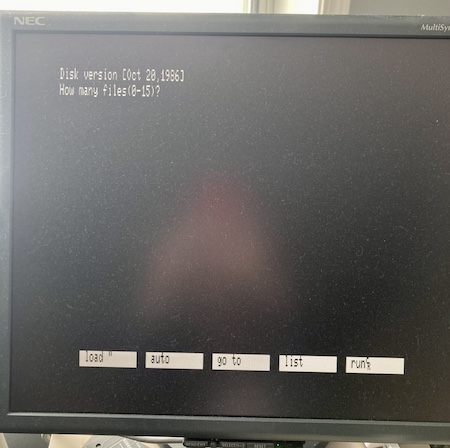
Although the initial video out was garbled (no doubt assuming 15kHz mode,) I eventually figured out a combination of resolution and options that made the 1970NX happy. Strangely, some of the higher resolutions caused the top line of the PC88’s video to double-up, which could be due to the weird height of the PC88 output.
Either way, the scaler was working. Now to clean up the job and make it look less like someone crashed a car into a Radio Shack.
Wrap-up
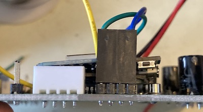
I clipped the Dupont connector off of the SCL/SDA wires, cut down the male pin header connector (I wasn’t going to desolder the ground pin again) and then soldered the wires down on the topside. To protect them and hide the ugly joints that resulted, I covered them in heat shrink and a bit of neutral-cure black silicone.
After that, the case went on fine. I had to go slow because the plastic fasteners would start to cross thread as they heated up, got soft and expanded, so no power tools. In the end of some finger-shredding hand fastening, I connected the whole assembly back up to verify it still worked on the PC88. The top plastic wasn’t particularly crystal-clear after it came off the sheet, but a little Novus will clean that right up. Or maybe it won’t, because it’s hiding some of my crimes against wiring.
I wanted to do a clock generator modification, which consists of adding a stable external clock generator based on the Si5351 chip to replace the original clock circuit for the scaler chip. Unfortunately, the Adafruit-branded experimenter’s board for the part was not available for purchase, and I couldn’t find any schematics for that board, so I had to go without for the time being. I’ll definitely add this in the future, as stable timing is essential for a good-quality sync.
Changing out the C11 capacitor for a larger-value one is also recommended on the wiki, as is adding some more bypass caps. However, I didn’t notice much noise, and I was in a hurry, so I left them as delivered. I also didn’t install a 100Ω pull-down on CSYNC as that modification is intended for game consoles, in order to approximate the 75Ω terminator of a TV. And I fully intend to use this with computers… and arcade boards… instead.
The power supply is a concern, of course – using the cheapo came-with-something-else AliExpress supply is likely to insert a lot of noise onto a board that isn’t good at dealing with it. We’ll see how that goes later; I might end up rigging up something to power it off the supergun’s power supply.
I also think it would be a cool idea to have done this mod with a “bridge-board” which sits above the GBS and has a nice place to mount the ESP8266, as well as exposing JP21, SCART, and Macintosh RGB connectors. Maybe even a switcher could be integrated. That would have been a much cleaner install, albeit still with a bunch of wires running everywhere.
For now, this teeny-tiny project is done. It’s nice to know that if my 1970NX dies, or if I take some of this junk on a road show when all of the current nightmare ends, I can finally use other LCDs around the house or on Kijiji. Time to finally put those lazy old 31kHz displays to work.