Make Your Own ColecoVision At Home (Part 1 - Design)
Tags: console coleco colecovision leako homemade-hardware homemade-software clone
When I found some cheap ColecoVision cartridges in the junk bin at the flea market, I knew I had to save them from whatever fate awaited them after the junk bin. How would I play them? Today’s old-ColecoVision prices are ridiculous, so I started building one instead.
Even though they made over 2 million of them, about the same number of US-market Sega Master Systems, there are some issues that seem to be cutting down the stock of old ColecoVisions kicking around:
- Triple-voltage “4116” DRAMs for the video chip (+5V, -5V, and +12V) mean that the DRAMs generate more heat than they really need to and then die prematurely - it also means a more complex power supply that will also fail;
- Failure-prone power switch ‘slider’ design that produces difficult-to-diagnose “kinda works” situations as it flakes out;
- Controller ports have poor ESD protection, causing damage to the decoders if you live somewhere with 1970s shag carpet or swap controllers often;
- Damage-prone motherboard substrate/solder mask that makes rework challenging;
- Generally enormous size means you might throw it out;
- Niche collector status that doesn’t have the name-brand of an NES or Atari 2600.
There are mods to fix at least three of these problems, but then you still have to secure a ColecoVision. And if I could do that easily and inexpensively, you probably wouldn’t be reading this article now.
At the time I started this project, the cheapest working ColecoVision I could find on eBay was $155 CAD shipped. Local classifieds were even worse: there was an untested ColecoVision for $500 and a boxed Adam for an eye-watering $1800. Speculators aside, this sets a pretty high budget for making a clone. Plus, I’ll learn something - and learning something is priceless. Especially if you learn it the hard way.
I had a few goals for this clone:
- Use composite video. There are a lot of ColecoVision composite mods, but if the TMS99x8 VDP is emitting composite video in order to feed the original RF, why not just do it right from the start? If I had been lucky enough to have TMS9928s in my junk bin, that would have been even better - enabling analogue RGB output like they had on European Colecos. Maybe in a future version…
- Try to keep the board size down. The original ColecoVision was a massive beast, not least because of all the power-management and RF circuitry that won’t be included on this board. I also wanted to use surface-mount chips where reasonable - they’re cheaper, more readily available, and will add up to a few saved inches of board space.
- Have an excuse to finally buy a ROM programmer. Yep, it’s gonna need a BIOS ROM for sure.
- Use a five-volt (or thereabouts) single-rail power supply.
- Try not to use any exotic or end-of-lifed parts other than the TMS99x8 VDP.
- Worry everyone around me by suddenly developing a strong interest in a relatively unpopular 8-bit game console.
Get on the bus, Gus
The big obstacle is that I didn’t understand memory decoding at all, or how a data or address bus works. I conceptually understood that inside an old 8-bit computer or game console, the CPU somehow addressed individual components, and then told them what to do or gave them some data. But I don’t actually understand how it works. This lack of knowledge felt like it was holding me back from doing cool stuff, like making expansion cards, upgrading the RAM in an MSX, or building my own single-board computer or RC2014 clone.
I couldn’t find a good explainer on the subject, after flipping through a bunch of introductory computer architecture textbooks and Intel service manuals, so I decided to start bugging everyone I knew around me for hints. At least for the ColecoVision’s Z80 - anything more complicated at this point would have probably killed me.
Eventually, I was able to piece some facts together, which I will now spell out in detail so you can keep up with the conversation at computer-engineer parties from 1982:
- The Z80 can access a whole lot of memory - it has a 16-bit-wide address bus, which is enough to directly map 216 = 65,536 unique addresses (or 64K of linear RAM.)
- The Z80 also has 256 I/O ports, which we saw previously when I tried to fix a broken PC-6001 volume knob through BASIC.
- Peripherals (usually) don’t know or care about the CPU’s memory addresses or port numbers: they need someone to come by and flip their “enable” pins when it is time for them to do their job. They might study a portion of the address bus, but only as much as they actually can take (e.g. the 8-bit “2114” RAMs on the original ColecoVision only have eight address pins.)
- Because only one chip on a bus is supposed to be “enabled” at a time (at least on the ColecoVision), everyone who the CPU directly talks to will share the same address pins (they are on the same address bus.)
- Peripherals are sometimes mapped into memory, which is to say they respond to a certain address. Since the peripherals don’t know what their address is, that’s the job of decode logic, which interprets the CPU’s requested memory address to figure out which chip to turn the enable pin on for.
- Same deal for I/O ports, but the ‘address’ is much smaller (only port numbers 0-255 are valid = 8-bit address) so you don’t need to pay attention to the top half of the 16-bit address when you are looking for an I/O port.
- You know when the CPU is looking for an I/O port, because the Z80’s
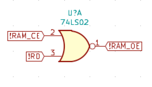
/IORQpin is low (the/means “active (when) low”). You know when you are looking into memory because/MREQis low. - If you use the “REQ” pin state, the address pin state, and the CPU’s read (
/RD) and write (/WR) pins, you can put together a bunch of basic logic gates into a combination that will let the Z80 write into a memory chip or any other peripheral you want!
I think because a lot of this stuff is sort of derived from knowledge you get in the previous step, nobody really writes it all down in one shot. Or maybe they’re just afraid of making a silly mistake in their explanation and looking totally stupid like I probably just did above (congratulations, you passed the test.) Hopefully, I’ve done my (very small) part to democratize an expensive engineering education by encouraging you to recklessly slap chips on a board and join like-named pins together.
Some Maps For These Territories
So if games on the ColecoVision are expecting peripherals to be at certain addresses in memory or I/O ports, how do we figure out where they are? Luckily, some anonymous genius has already documented the memory map and the I/O port map for the CV in the ColecoVision FAQ that once lived on Usenet:
Memory Map
0000H - BIOS ROM
.
1FFFH

2000H - Expansion port
.
3FFFH

4000H - Expansion port
.
5FFFH

6000H - Start of RAM (1K mapped into an 8K spot)
.
7FFFH

8000H - Cart ROM (broken into 4 sections, each enabled separately)
.
FFFFH
I/O Map
00-1F - No Connection
20-3F - No Connection
40-5F - Video
60-7F - Video
80-9F - No Connection
A0-BF - No Connection
C0-DF - Sound
E0-FF - Controllers; E2 is special, as well as E0 - E0 appears to be the readback, and E2 appears to be the scan - 39
I’ve copied these verbatim. If you are the actual author of these maps, I’d like to shake your hand and also credit you.
Those addresses seem pretty round - let’s look at the binary for those addresses to see how many bits of the address bus we’ll have to care about in order to decode them. I wrote a quick little Python program to convert them from hex to binary, and also pad the output, because despite my interests I am still not great at converting hex to anything:
def to_bin(h):
    return format(h, '016b')

def walk_map(m):
    for (start_offset, identifier) in m:
        print(to_bin(start_offset) + ' ' + identifier)

memory_map = [ ( 0, 'bios rom' ), ( 0x2000, 'expansion port' ), ( 0x4000, 'expansion port' ), ( 0x6000, 'start of RAM' ), ( 0x8000, 'cart ROM bank A' ), ( 0xa000, 'cart ROM bank B' ), ( 0xc000, 'cart ROM bank C' ), ( 0xe000, 'cart ROM bank D') ]

io_map = [ ( 0x40, 'video' ), ( 0x60, 'video' ), ( 0xc0, 'sound' ), ( 0xe0, 'controllers' ) ]

print('Memory Map:')
walk_map(memory_map)

print('I/O Map:')
walk_map(io_map)
The result:
Memory Map:
0000000000000000 bios rom
0010000000000000 expansion port
0100000000000000 expansion port
0110000000000000 start of RAM
1000000000000000 cart ROM bank A
1010000000000000 cart ROM bank B
1100000000000000 cart ROM bank C
1110000000000000 cart ROM bank D
I/O Map:
0000000001000000 video
0000000001100000 video
0000000011000000 sound
0000000011100000 controllers
Looks like only the upper 3 bits change on the address. This means that our decoders will only need to care about A15, A14, A13 when decoding memory, and A7, A6, and A5 when decoding an I/O port request.
I scrawled out this truth table, because I dimly remembered making a truth table in my undergraduate hardware class in univesity computer science. Turns out all that stuff eventually came in handy!
| A15 | A14 | A13 | Decodes to peripheral |
|---|---|---|---|
| 0 | 0 | 0 | BIOS ROM |
| 0 | 0 | 1 | Expansion port |
| 0 | 1 | 0 | Expansion port |
| 0 | 1 | 1 | RAM |
| 1 | 0 | 0 | Cartridge, bank A |
| 1 | 0 | 1 | Cartridge, bank B |
| 1 | 1 | 0 | Cartridge, bank C |
| 1 | 1 | 1 | Cartridge, bank D |
Same deal for the I/O:
| A7 | A6 | A5 | Decodes to peripheral |
|---|---|---|---|
| 0 | 0 | 0 | - |
| 0 | 0 | 1 | - |
| 0 | 1 | 0 | Video |
| 0 | 1 | 1 | Video |
| 1 | 0 | 0 | - |
| 1 | 0 | 1 | - |
| 1 | 1 | 0 | Sound |
| 1 | 1 | 1 | Controllers |
I assume other computers must be way more complicated, but the ColecoVision’s memory map is nice and simple. Thanks, anonymous engineers who took some time off from making Cabbage Patch Kids to scrawl out this memory map.
Mux On, Mux Off
In fact, it’s so simple, that the original developers just used two 74LS138 demuxers. What these chips do is turn your 3 1-bit address values into one of 8 outputs through the magic of whatever happens inside there.
You can also toggle 3 bits of enables from there, of which E1 and E2 must be active but E3 cannot be in order for the demuxer to work at all. The third enable bit is sort of a ‘handbrake,’ but the ColecoVision uses it to cut out the internal decoder when you attach an external device (like an ADAM) that has its own decode logic.
I pretty much just copied down what Dan Boris did in the schematic, and then tried to understand it later. The result looks exactly like my truth table up above! It’s almost like other people have been designing computers for decades, and a lot of parts already exist to help them do it…
One small wrinkle was that the replacement SRAM I picked - a bag of 5V-tolerant Sanyo LC331632M-12 64KB chips that were intended to repair a JVC X’Eye a long time ago - had an OE pin, whereas the original 2114 SRAM did not. With a quick little bodge, I ran it off of the combined efforts of the chip-enable for the RAM and the “read” signal from the Z80. At least now I can say I designed one of the gates on this thing, even if it did introduce a NOR chip that nothing else used.
Update: This actually did the opposite of what I wanted it to do.
With the memory and I/O decode worked out, it was time to move onto the TMS9918 video chip…
Vid Kid
Unfortunately, the TMS9918 video chip has been designed to work pretty closely with eight 4116-style 16Kbit DRAMs. They’re not uncommon right now, but I don’t want to put eight of them on my board, especially when I have a bunch of perfectly good 64K SRAM chips right here. Fortunately, a guy called Tom LeMense already figured out how to convert a TMS9918 to use SRAM, so I ripped off his design wholesale.
Tom basically uses a few flip-flops (think one bit of memory) to intercept the odd-ball addressing scheme that the TMS9918 uses for finding its RAM, and then convert that scheme into something that one large SRAM like mine can understand. The whole thing made my head swim, especially when it gets into using the propagation delay from a signal going through multiple inverters to tune the row-access timing.
Of course, more gates and inverters were added, but I still came out net ahead on chip count from this portion of the machine. It’s worth pointing out that the TMS9918 does not expose its memory to the CPU: the Z80 interacts with it through an I/O port, and then the 9918 has its own separate memory bus for messing with the contents of its video memory. I was happy to save some complexity here, and it’s nice that so many people have tested them. As a side bonus, his schematic also produced a workable composite video output circuit. Thanks, Tom!
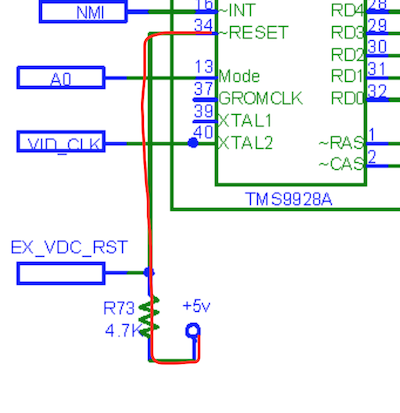
It was a little weird for me to discover that the TMS99x8 is not reset by the CPU, as I assumed every peripheral would have to be. If you don’t have an expansion device (e.g. an ADAM) to reset it for you, it ain’t getting reset! I guess the BIOS must do all the initialization and doesn’t want to be overruled. This lack of a reset was so surprising to me, that I had to confirm it with another set of schematics of the ColecoVision “Delta” board inside an ADAM.
As an aside, you might notice that the schematic says TMS9928. The TMS9918, as far as I can tell, has virtually identical features to the TMS9928 other than not being able to output RGB (via YCbCr,) and it’s more widely available - probably thanks to being included in every MSX1 that ended up in a Chinese scrapyard. If I ever have to move to a TMS9928 (because maybe I misread something), then it will probably require a board rework as the pinout is a little different and I would have to make a composite output circuit, but that’s an excuse to do an even smaller version in my book.
Watching the Clock
I have a friend who has some sort of pathological hatred of clocks. Without a further explanation, I have to assume this fear originates from some kind of last-minute project in his electrical engineering class that just didn’t go right. Me, I love clocks. I love their little hands, I love the tick-tick sound they make.. CPU clocks? Oh yeah, I guess I could like those too.
The original CV uses a 7.15909MHz crystal, which is hard to get new (DigiKey had a few vendors, but they were all non-stocking). They have a lot of 14.31818MHz crystals, so I devised my first-ever clock divider.
The way a clock divider works is to pass your original clock through a flip-flop. The flip flop changes its value only half as often as the clock does (because you feed the last value stored into the ‘set’ pin and it only actually gets set on the rising edge of the clock) so you end up with an output from the flip flop that changes only half as often as the clock going into it does.
It took me a long time to try and understand it, even though a prof had explained it to me in my university hardware course a long time ago until it sunk in. The Germans probably have a word for knowledge that you thought you didn’t have that you were actually taught before and just didn’t internalize.
Part of what helped me finally realize that it did work was to run it in a circuit simulator. If you want to try it for yourself, I prepared a test project in that circuit simulator.
Since the CV’s Z80 and sound chip run at 3.57MHz, there was already one clock divider to go from the original 7MHz clock. All I did was stack another flip-flop in front, so technically the 14MHz is getting divided by four to feed the CPU and SN76489.
The clock is also multiplied by three in some way I don’t quite understand yet to produce the 10MHz the TMS9918 expects (and is very picky about, as producing television colour requires exact timing). Only actual testing will tell if the resulting clock signal is clean enough for the newer PLCC Z80, or if I need to redo the whole clock section, possibly with something expensive-but-easy like dedicated programmable oscillators.
Control Yourself
As stated multiple times already, the original ColecoVision power rails are +5V, -5V, and 12V - about what you’d expect to run the triple-voltage DRAMs for the VDP. Part of the benefit from substituting a more modern SRAM for those DRAMs is that I would be able to simplify the power rails to just +5V. However, the controller decode logic still needed a “pull-up” to -5V, as shown here on the schematic:
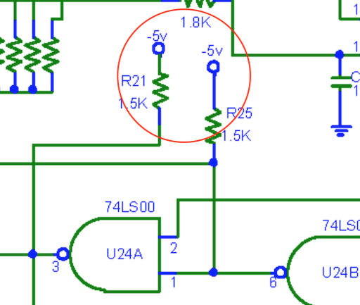
While this is probably an optimization (whomever did the clock circuit and controller decoding is extremely clever), after a few evenings of staring at it and running it in a circuit simulator, I was unable to really understand what was going on. So I just copied the entire whack, but now I needed -5V. Where was I going to get it from?
A couple months ago, I found out about the TI TPS60403 “voltage inverter,” a magical little SMD (5-pin SOT-23 for ‘easy’ soldering) component that can take any voltage from 1.6V to 5.5V and produces the negative version of that through some kind of wizard magic. Hey, I’ve already got a TI video chip, maybe they will be friends. Obviously, this chip can’t deliver boffo amounts of current (it’s topped out at around 60mA,) but that is probably enough for these two logic gates. It did balloon my parts count, and it doesn’t come cheap, but it’s also a lot cheaper than adding a dual-voltage power supply.
For the sake of laziness, I decided not to build my own ColecoVision controllers. They’re not hard to build, but I’m also not super willing to go back into keyboard matrices so soon. Feels like I’ve been having a lot of that kind of thing lately. There’s also the problem of sourcing a case - injection moulding is both expensive and an entire new area of obsession that I don’t need to get into right now. Maybe I’ll chop up one of the Aliexpress “Not a Nintendo” Famicom-looking USB controllers at a future date.
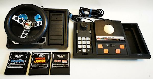
I managed to scavenge some loose controllers off of eBay for $7.50. One battered regular controller, one Roller Controller, and one steering wheel expansion module joined my parts pile, along with some games which support neither of the fancy controllers.
The shipping on this lot cost more than it should have, the Roller Controller needs a proprietary power supply, and it’s a little hard to justify storing a massive corrosion-prone steering controller that I can’t use with my lack of an expansion port, but it will be nice to have a known-original part to test against.
If nothing else, getting the Roller Controller to work will be a cool project. I never had one before, and didn’t even know it existed prior to starting this project. Maybe it will make Omega Race all that much sweeter.
Putting it Together
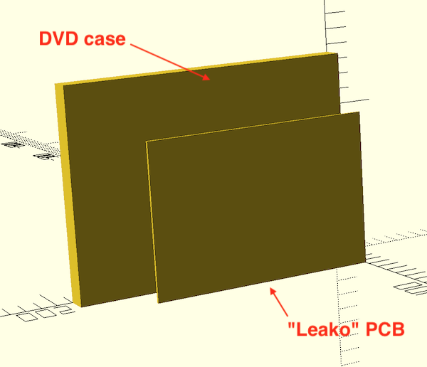
With the schematic half-copied and half-fabricated, I could finally begin the fun part - routing. At this point, I expanded the board from 100x100mm to 150x100mm so I would have enough space to fix it if something went wrong with the first design. 150x100mm is still quite a bit smaller than a 190x135mm DVD case:
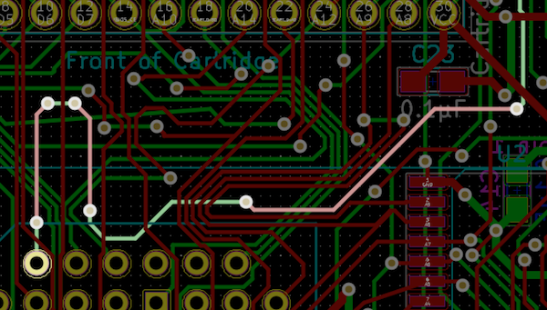
Making the board bigger also made the routing easier, but not as easy as you’d expect. The space in between major components to run the address and data buses is still limited, so I ended up with a lot of vias. The CPU clock trace is particularly ugly, running from the clock generation circuitry up by the BIOS chip all the way down to the CPU:
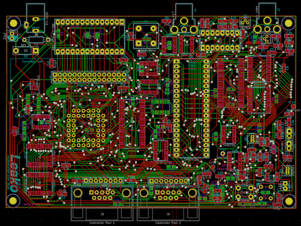
I’m not sure what the technique is to better plan out this kind of thing - it is probably one of those skills that grows with experience and knowledge of “what not to do.” I usually just watch the ratsnest wiggle around when I move the ICs, try to straighten it out as much as I can, and then hope for the best as more components are added on later.
I made sure to add a bunch of decoupling caps to every IC - it’s better to have them than to not - although they did end up in weird places that are going to be hard to solder. On the plus side, With a total of 41 SMD 0805 capacitors and 44 0805 resistors, I’m going to be getting really good at surface-mount soldering.
After about two weeks of mornings and evenings, I had my first version of the board ready to go. It’s extremely beautiful from above:
Let’s see where we’re at on hitting the budget:
| Item | Cost per unit (CAD) |
|---|---|
| PCBs | $5.56/ea ($27.82/5pc shipped) |
| New parts (Z80, sockets, passives, 74 logic) | $53.60 |
| TMS9918 (Aliexpress) | $1.97/ea |
| Sanyo LC331632M-12 RAM | $5.69/ea |
| SN76489AN sound chip | $0.45/ea ($2.24/5pc shipped) |
| 27SF256 EEPROM | $1.26/ea ($12.59/10pc shipped) |
| DE9 controller ports | Free from a junk pile |
| Total price | $68.53 |
The three most expensive “new” parts from Digi-Key were the following:
- 10MHz 44-pin PLCC Z80: $7.64
- Card edge connector for cart slot: $6.01
- 14.31818MHz oscillator: $2.52
Not bad. Of course, this doesn’t include my labour, diagnostic time, or any future revs of the board I might have to make. And all of the ‘old parts’ are going to become more difficult to find in the future and correspondingly more expensive. Most of them are probably scavenged from e-waste, and thus unreliable for a large-scale production. Luckily, I’m not doing a large-scale commercial product out of this: I just want to satisfy my urge to get a ColecoVision for less than the price of a 1993 Honda Civic.
I will still need to buy a ROM programmer (most likely a TL866) to write the BIOS ROM, which is a tool that I’ve always wanted but never really had a solid justification for getting. That will of course increase the total price of this project, but it’s something I can use again and again, so I’m not going to count it.
The board will need some way to stay off the desk, especially now that it has components on both sides. I haven’t worked out a method for that yet, but the “M3” holes that have been cut into the board should provide me at least with a simple way to put some standoffs in.
Q&A
I’ve had a couple questions from friends and acquaintances when I’ve brought up the project, so I’ll try to answer them as well as I can while I wait for the boards and components to arrive.
Q. How long until the next update?
Right now, because of the Coronavirus situation in China, the fab I chose (JLCPCB) is running behind schedule. It will probably be more than a month from now until I get the first board in my hand. And I also have to buy some equipment (the aforementioned TL866,) which will also come from China and take about the same amount of time.
In the next update, I plan to at least solder the board together, which will take a bunch of time as well. Of course, if I find out between now and then that I made a bonehead move and have to re-order a fixed board - really the best case - it will take some additional time. And I’m doing this for fun, so I don’t try to hold myself to timelines. It will all happen when it happens.
Q. Will it have ADAM compatibility?
Not yet. I’ve axed the entire expansion slot to save some board room, which might have been a mistake since I could have used it for some kind of test jig. However, I’m unlikely to make that test jig, and the expansion slot also produces 12VDC, which the ADAM needs.
I might do a later rev of this board and add on the ADAM stuff, but I would have to understand it a whole lot better than I do right now. All I can tell so far is that it takes over the I/O and RAM decoders in “ADAM mode,” and provides some extra stuff. I also don’t have any non-tape ADAM software, and the tapes themselves are hard-sectored, which makes the whole project much more complicated.
Q. Will you sell these?
Probably not. The BOM cost alone is pretty high, and my labour to assemble them would have to push it into the stratosphere. I don’t even know if this will work when I put it together; it could very well be another couple of months until I have a working version. Maybe if it works I could partner with a manufacturer to produce them, but the supply constraints of relying on “used” RAM, 80s video chips and 80s sound chips are a realistic limit on how many of these could ever be made, much less in large enough quantities to cut the BOM price.
I’ll probably open up the GitHub repository once I have a working board, so if you’re really interested you could make your own from my Gerbers.
If there are a lot of bum boards, people I know are going to end up with one to hang on their wall. I wonder what “real” engineers do with their scraps.
Q. What’s on the wishlist after this works?
“After this works” is a pretty distant point in the future, but assuming that the gods of the Connecticut Leather Company smile upon me, it would be cool to use this same board to make other clones of similar computers:
- Sega SG-1000/SC-3000;
- A generic MSX1;
- Coleco ADAM
Another very cool direction to take this in would be a portable system. If I could make the board even smaller and less power-thirsty it would be a cool little machine to take on the go with you. However, that would involve a lot of case-manufacturing, LCD-figuring-out, and battery management, so that would be a pipe dream for sure.
What’s relatively easy now that I understand more about how the system works would be to make my own ColecoVision multicart. The AtariMax SD-card “flash” cart seems like a great product, but I would like to build my own to verify my understanding.
If I do build another small computer or console clone, I think at this point it would probably either be a PC-6001 or a CoCo clone. Both of those have an MC6847 video chipset, but two wildly different processors. The CoCo in particular would give me a chance to play with the Hitachi 6309 “6809 on steroids.”