Make Your Own ColecoVision At Home (Part 2 - Assembly)
Tags: console coleco colecovision leako homemade-hardware clone
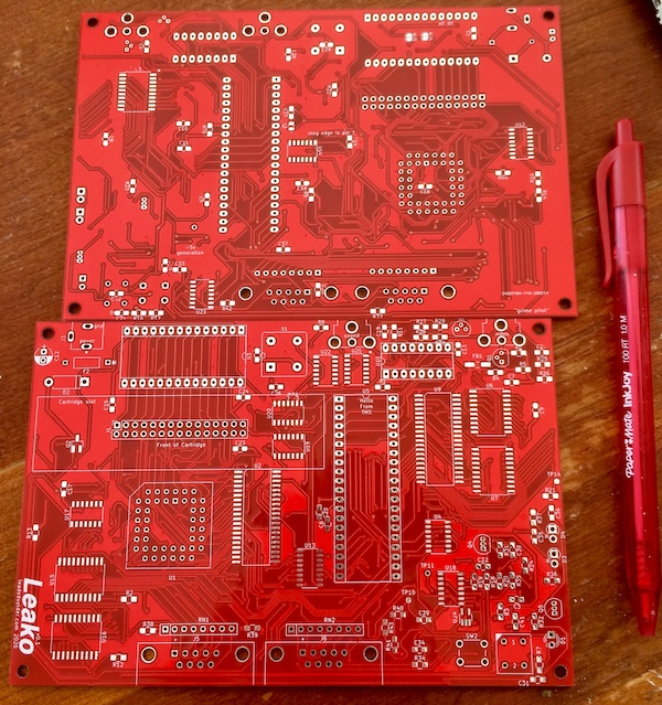
The boards for the homemade ColecoVision clone project have arrived. It’s been a long haul of finger-burning fun to get the console assembled, but will it ever be able to play a cartridge?
Parting, with Cash
Almost immediately after the Gerbers were sent off to JLCPCB, I ordered the entire BOM from Digi-Key. A huge bag of crap arrived within a few days.
It’s easy to lose scale on how big things really are when you’re constantly fighting for those fractions of a millimeter to route traces. At human-scale, I was a little shocked by how small a lot of the components were. All the SOT-23 stuff is smaller than a pinky fingernail and has teeny-tiny pins that don’t stick out very far. There’s no better way than this to get better at surface-mount soldering!
There were a couple problems with the order, but that’s to be expected. This was definitely the biggest parts-count board I’ve ever done, and I learned a lot. Things like, don’t leave making the BOM until the very last minute, because it takes an entire morning and four cups of coffee. And that you should always do the BOM before you order the board, in case your footprints aren’t right.
One big problem was that I wasn’t able to find a bi-polar 68µF capacitor in 0805. You’d think that would be easy, but it appears the laws of physics forbid it. I changed the footprint (after ordering the board, of course) to a larger 1206 and then ordered some through-hole ceramic caps that I could bodge onto the pad. Said 68µF capacitor is for the clock circuit, so I think its value was quite important:
You might be asking yourself why I need such a big capacitor for a clock circuit. Aren’t clock circuits usually using pico-Farads? Well…….
A few hours after I ordered the parts, I got an email from Digi-Key saying that there was an inventory discrepancy and that they actually only had one 2kΩ 0805 surface-mount resistor in stock, not two. This was a pretty funny idea to me, that their inventory robots would constantly be shuttling past a sad bin that only contains one minuscule resistor in an extremely common capacitance.
What was even funnier is that the part was now discontinued - as if a bunch of people working at the resistor factory got told by their boss that he doesn’t think anyone’s going to really want 2kΩ resistors anymore. “No, what customers want now is capacitors,” he’ll chuckle at his business acumen, while the resistor department’s hated rival, Bob Dielectric, rubs his hands in glee. I ordered literally one hundred 2kΩ 0805s from a different manufacturer for a buck instead.
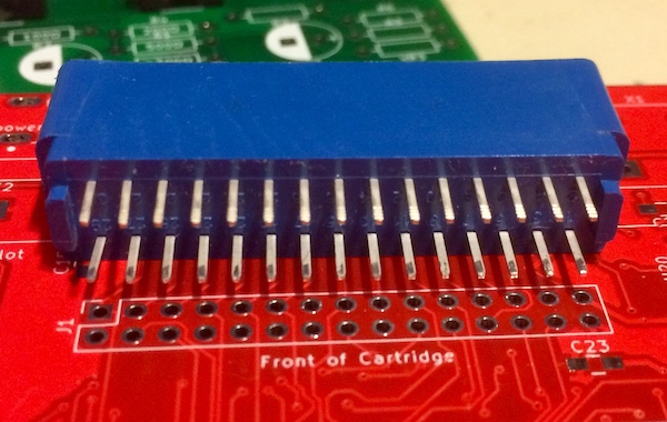
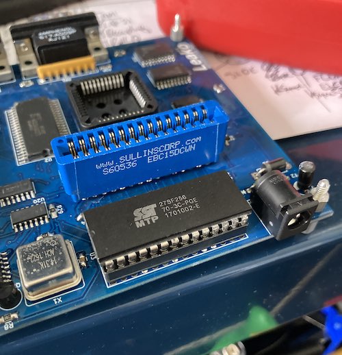
What’s not as funny is that the cartridge slot I had paid six bucks for came without pins. When I saw it on Digi-Key, it had been listed without an image, but I figured there was no way it wouldn’t come without pins. After cursing myself, I ordered up another bunch of 0.1” 30-pin edge connector slots, except this time with pins. The new Sullins-branded ones came in a fetching shade of blue and - just to rub it in - cost a little less. However, they still weren’t what I was looking for…
Another small opposition to the project came in the form of some local scumbag, who stole one of the DigiKey orders off my porch, tore it open, presumably found nothing that they could fence or snort, and then threw the opened box into my backyard. Everything was still there, but clearly the forces of “I’d really like some drugs” are aligned against the Leako Initiative.
And, yes, the clock circuit did ask for 68 pF. I made a mistake reading it off the schematic, which changed between notations of capacitors depending on which sheet you were looking at. I figured this out a while later, which I’m not very proud of.
Sound Off
Another mistake I made was not reversing the data bus on the 76489 sound chip. Like the TMS9918, this TI sound chip is also ‘backwards’ from the Z80’s data pin convention: pin D0 on the Z80 goes to D7 on the 76489 and so on.
I resolved to bodge wire this onto a piece of protoboard, and just live with the shame for now. Unfortunately, the sound chips took several months to arrive (coronavirus again,) so I ended up just going ahead with the v0.2 board, where I made this change. Despite the counterfeits and recaps, it is great to ride the “80s grey-market sound chip” market until something like this happens to screw it up.
When one of the orders of SN78649s arrived, I built a breadboard tester for it powered by an Arduino. I had heard that the reliability of these chips was very low, so I expected not very many of them would work. The first chip I tested worked great - except that my code was terrible and didn’t produce a reliable result due to bad timing.
After a few hours of bodging and reading documentation on SMSPower, I managed to figure out how to test the chip. Here it is cycling through channels 0, 1, 2 and the two kinds of noise supported by the chip. At least we’ve got one known-good salvage part!
Controller Prep
The controller I ordered as part of a lot from Quebec in the previous entry arrived almost immediately, and I set about tearing it down and cleaning it. It was really gross! The plastics got washed in my kitchen sink, the coiled cord scrubbed with the flossing method, and the (delaminating) matrix keypad got a once-over with some disinfecting wipes.
It had one missing coarse-thread Phillips screw, which I replaced with another from my junk drawer. I still haven’t figured out how to get a new shiny ‘grip disc’ for the top of the joystick - maybe I’ll make something with hockey tape.
Cleaning and servicing controllers doesn’t need a whole lot of focus or technical skill, which makes it the perfect task to say you’ve actually done something on a project today.
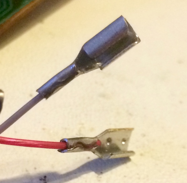
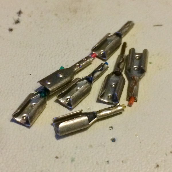
The wires that go from the DE9 cable onto the PCB are just crimped onto the pads on the PCB. A bunch of these crimps were super loose and probably not making good contact, which might be the reason why this controller was getting sold with the other junky parts. I tried to tighten them up, but one tragically snapped as soon as I applied any force:
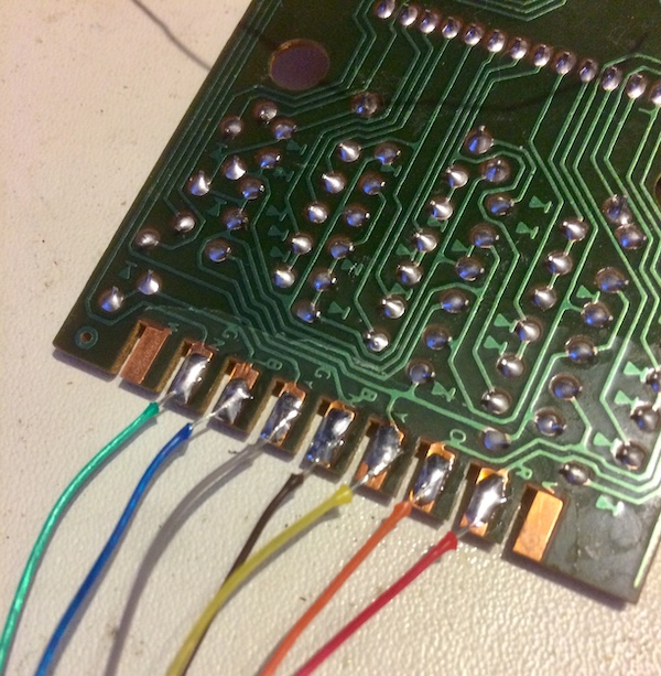
I decided I would cut off all the crimps and solder the wires directly to the board. This worked okay, except that the insulation on the wires was definitely not solder-heat proof and melted. Since the pads had never been used for solder in 37 years, I decided it would also be prudent to put a little liquid flux on them in order to prep them for the solder.
The joints weren’t pretty since I had to work fast. That’s my excuse. Also, I had to desolder the entire thing and do it again after I realized the wires have to slip through the back plastic case and so should be soldered only after threading them through…
Finally, after some fighting, I was able to reassemble the controller. It wasn’t a great fit, even with the new screw, because the lower plastics that clip together had broken from age and abuse. Also, I didn’t do a great job of actually cleaning the top plastic for fear of rusting the spring, so I went back and did another quick scrubbing with a q-tip and isopropyl alcohol.
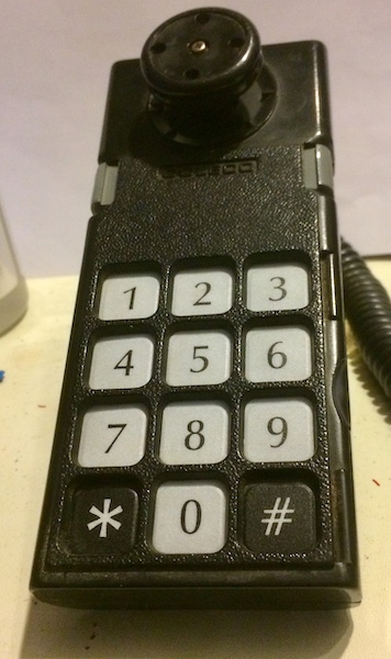
That was a lot of work for an ugly controller that doesn’t feel that great in the end… I hoped it would at least work. I can always buy or build a nicer one later.
Get Onboard
Eventually, the boards shipped from the fab. One of them had been ‘scratched’ during the assembly process, so I was fully refunded on it. It’s still nice enough to use for a practice board in the future.
And as soon as they shipped, I noticed something a little weird. Remember last episode, where I told you about how to wire up a clock divider? Well, the new clock divider I added to go from 14MHz down to 7MHz was done correctly, but not the “original” clock divider from the schematic that I blindly copied.
Here are the two dividers in different schematics:
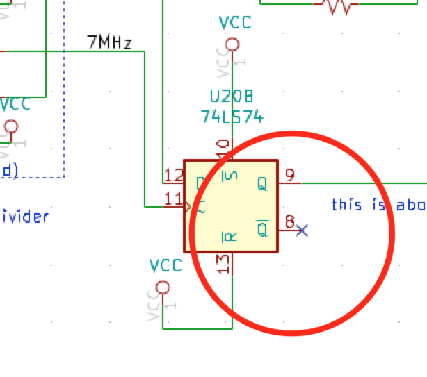
The latter schematics, by an Atari Age user known as ChildOfCv, were meticulously double-checked. Had I known there were errors in the original schematic, I probably would have gone from the start with ChildOfCv’s. I have a huge debt to the original schematics, of course, as that is an immense amount of work. One or two errors here isn’t surprising in a task like that. It was only here that I discovered my 68pF clock circuit error, in case you’re keeping track.
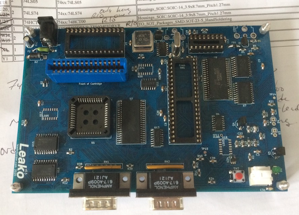
Clearly, it was time to rework my clock circuit and spin a v0.2 with all the other problems I’d noticed. This made the board a little uglier in some spots, as I tried to reintroduce chips into the same general location they had once occupied but ran new traces. My timing circuit got split up when I put it on the board originally (since I left it for almost last), so changing it isn’t necessarily a matter of removing one chunk of the board and laying a new one down. I’ll try to get better at keeping physical space for “zones of responsibility” on future projects. Still, though, the re-routing took less than an hour and I was able to send the v0.2 board off:
Why yes, I did put Q3, a through-hole transistor, right in the way of the plastic shell of the cartridge when it is inserted into the slot. Good thing they have bendy legs…
v0.1 Arrives
Even though I knew that my first-born clone board had some flaws, it was hard not to smile when I unpacked the boards. They’re so tiny, but they (will) do so much!
That RAM chip next to the Z80 being so far north really bugs me now, although I hardly noticed it before. If it works…
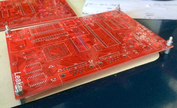
I used some of those little jackscrew standoff retainers that hold on VGA cables to stand the board up off the table. This is important not just for looks, avoiding shorts, and cooling, but because there are chips on both sides. They weren’t a perfect fit for an M3 hole, but when screwed tightly together they don’t wobble. At last, the junk-bin investment is paying off.
Even though I had already ordered the v0.2 boards, I started doing some of the test-fitting that I should have done on paper. That’s right, I’m once again re-learning the lesson that printing out boards is basically free but reworking them is pricey. In my defense, the ancient HP LaserJet I own takes long enough to start up that it might actually be a little faster to order boards from China.
There were a few big mistakes.
Mistake #1: Cartridge Racer
By far, the most obvious mistake is that the replacement cartridge slot is spaced wider apart than the actual holes in the board.
I had used a simple 2x15 pin header footprint, thinking that the rows of pins would be only 0.100” apart, but in fact they were 0.200” apart, because there was a missing row in between. They’d still fit on a breadboard, but my board footprint was wrong enough that I couldn’t just slot the cartridge slot in. This is another one of the footprint mistakes where I should have printed the damn board out first.
I ended up making a new footprint for v0.3, which I definitely checked with a paper printout this time.
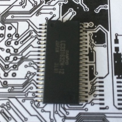
In the course of test-fitting, I realized that I had completely forgotten where the Sanyo RAMs I had bought for Genesis repair got off to. They used to be shoved into a corner of my workbench drawer, but as space became tight there, I figured I should move them somewhere safe in order to protect them from an errant ESD-laden elbow or fumbled soldering iron. After a few hours of fruitless searching, I decided to check the meticulously-organized component storage bins that I never put anything in. Which is of course where they were.
Mistake #2: The Power Switch
I wasn’t provided with a footprint for the power switch by the manufacturer, so I made my own. And apparently, their datasheet and the actual switch disagree on which pins do what (luckily the dimensions are 100% bang-on). I thought the “top” and “bottom” pins were the two sides of the switch, but it is actually the “left” and “right” sides.
After continuity testing, I realized my mistake, and removed the switch and bent the leads with a pair of pliers until they could be fit into the rectangular holes at a 90° rotation. It didn’t look good, and the height of the switch made it very awkward to flip over the board to solder on the backside. I should have left this part until the very end of assembly, but now it actually switches on and off.
The reset switch was also wrong, because I ordered a surface-mount button instead of a through-hole variant, but I also had a huge pile of tac switches lying around anyway. Kids, take this lesson to heart: that’s why you hoard.
Mistake #3: The wrong footprint for the RAM
There’s a downside to hoarding too, of course. Remember how I said earlier that I couldn’t find the RAM? It turns out the RAM has J-leads and the footprint I picked on the board does not. This meant that the RAM’s legs were simply too wide for what the board was expecting, so there was no way I could solder to it.
Update: The RAM actually has a gull-wing lead. The footprint I picked was a J-lead.
I kind of wish I hadn’t left this until the very end, but it is what it is. With this big of a mistake, I was basically stuck with having to do a re-spin. I could live with bodge-wiring the cartridge slot, but not two surface-mount 40-pin RAM chips.
I definitely printed out the footprint this time. Good thing, too, because it took multiple iterations of footprint adjustment until I got a nice one:
The KiCad footprint wizard is not at all obvious when you are putting in dimensions for legs. You also can’t use the caliper tool for measurements inside that editor, so you have no idea how big any dimension in the footprint actually will be until it comes out. Or maybe I just can’t figure out how to use it properly. Either way, a pretty frustrating iteration that would have been much worse if I had been re-spinning boards without printing them out first. Paper is cheap!
Mistake #4: Right footprint, wrong symbol
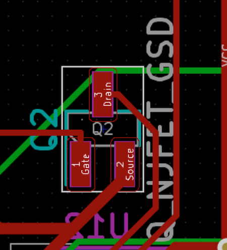
When I had partially assembled the board and went to test the power supply, I was disappointed to find it didn’t work. The reason is because apparently FETs are not all the same pinout!
KiCad contains six different N-JFET symbols, and the power FET I chose did not line up with the default (DGS). I made a “TODO” note to check it against the data sheet, but didn’t actually bother to follow up on it before fabrication.
I bodged it on the test boards, and adjusted the footprint in the “next board” branch in the repo. I also added some really explicit net labels to the schematic to make sure I don’t mix it up in the future:
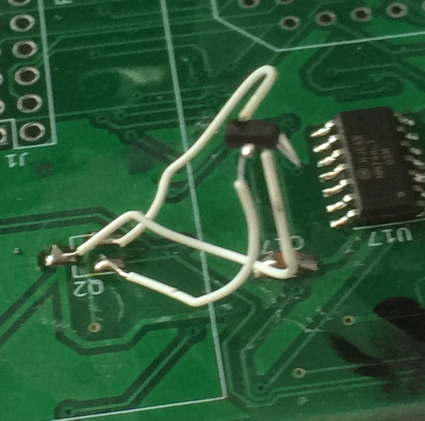
This turned into a bit more of a debugging adventure as I was first not seeing the power LED turn on (it was in backwards) and then not seeing any voltage at the chips even though the FET was operating.
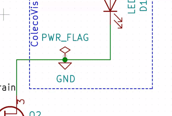
My super smart friend Scott figured this out within about five seconds of looking at my schematic: the GND pin was never actually attached to the “drain” line, just lying near it, and I didn’t notice a disconnected GND lying in the middle of nowhere as a problem on the electrical test.
Once the power was re-attached, there was good news and bad news. The CPU clock was a solid 3.579MHz, so all that clock division is working great.
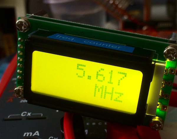
On the other hand, the TMS9918 video clock, which needs to be at an excruciatingly precise 10.738635MHz +/- 0.005%, was showing up on the board as only 5.6MHz with a bunch of drift.
Mistake #5: The wrong pinout for the Z80
I used KiCad’s built-in Z80 symbol when I was first laying out the schematic, and never went back to confirm it. Of course, the built-in Z80 symbol is for DIP, and I am putting a PLCC Z80 in mine. The pinout of the two chips are nowhere near close (PLCC A15 is pin 44, whereas it’s pin 40 on the DIP,) so it’s probably a good thing I never fired it up.
I wish I had caught this one before sending v0.3 to the fabricator for the first time, but I only figured it out that evening when I was experimenting with a new schematic for a different potential Z80-powered project. “Hey…”
Oh well, it’s just money…
Smaller mistakes: assembly idiocy
There were a couple circumstances in which I accidentally put C38 into R38 and vice versa, or put a 74LS04 into a slot meant for a 74LS74. I think I caught all of these - at least they were on the v0.2 board, which never fired - but it got me thinking about how I could help avoid this in the future.
Some ideas for process improvement here:
- Use different footprints for resistors and capacitors. I think I’ve seen this on other professional boards. If you’re trying to solder an 0805 resistor into a spot meant for a 1206 capacitor, then you’re going to notice right away. I have not done this for v0.3, because it is hard and would require me to re-buy my parts, but any future board of any complexity is definitely going to get it.
- Mark the actual chips on the silkscreen. I did this for v0.3+, since it was easy.
- Print out the BOM instead of looking at it on a monitor, so I can cross it off with an actual pen like some kind of caveman. I did this for later boards, which sped up assembly a lot.
- Pay the extra money for fast shipping, and use the extra week before submission to thoroughly double-check the board. $10 more for shipping is a lot less than $30 more for a new spin + cheap shipping again. I did not take this advice. If I had caught the Z80 footprint problem at this point instead of immediately sending the board out after verifying the footprints physically worked, there wouldn’t have been a v0.3 at all.
Lots of good lessons to be learned here. I just wish I hadn’t spent a few days soldering before I learned all of them:
Still though, look at it. It looks like a real, actual computer thing! That’s pretty cool on its own.
Third Fourth Fifth Time’s The Charm?
By being impatient and ordering before taking my time to double-check my work on paper, I blew through the v0.3 and v0.4 re-spins of the board. I realized that the Z80 footprint was bad only about ten seconds before the v0.3 board had been “approved for production” and could no longer be cancelled, so they ended up arriving together. At least I saved a bit on shipping the second board.
Here’s a short list of the revisions and what I fixed in each.
- v0.3
- Cartridge slot (Mistake #1)
- Rotate power switch (Mistake #2)
- Wider pads for the Sanyo SRAM (Mistake #3)
- Wider footprint for the transistors so I don’t have to bend them
- v0.4
- Z80 CPU pinout (Mistake #5)
- v0.5
- Fix power-FET footprint (Mistake #4)
- Hook up switched ground to logic ground, so the console will actually turn on (also Mistake #4)
- Use this rewire just in case the SRAM I’m using for video RAM is too slow
- Beefed up power and ground traces where I couldn’t fit the plane pours
- Get rid of about fifty vias, just by doing better wiring, flipping some caps to the backside, and using the planes properly
- Remove the crazy “harmonic clock multiplication” for the TMS and just spend a buck to add a dedicated 10.7…MHz crystal to the board
Phew! That was a lot. Unfortunately, while I was making these boards, cheap shipping from China became no longer available due to the onset of the COVID pandemic. This meant that the cost of every re-spin more than doubled, especially after getting soaked for customs “clearance fees” by DHL and UPS.
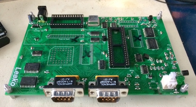
At last, the v0.5 boards arrived. I was really looking forward to soldering these bad boys up, not least because the previous board stuffing (and PC-9801NS/T surface-mount cap-replacement-palooza) had sharpened my skills considerably.
The big improvement to assembly speed on this build of the board was that I actually printed out my BOM, instead of looking it up on a screen. This way I could tick off parts as they are installed, make notes for bad footprints, and mark down when I’d used the last of a value of resistors or caps. Paper’s cheap.
When I put together the v0.2 board, I realized I had ordered a ‘wide’ 74LS05 chip instead of a ‘narrow’ one like my footprint on the PCB used. I made a note to order the narrow chips, but I guess I didn’t actually follow up on that note in the intervening months.
I ended up waiting to do another DigiKey order, because spending eight bucks to ship three dollars’ worth of chips just didn’t make economic sense. And my TL866 still hadn’t arrived from China. I considered desoldering the chips from the v0.2 board, but I also was waiting on a heat gun, and ended up destroying an SMD 74 chip the last time I tried to desolder it.
BIOS-Fest 2020
Once the board was together, it was just a matter of waiting for the TL866 EPROM programmer to arrive. I let this project take the backburner while I did a few more repairs and then a couple after that too. I also started a bunch of new projects in the meantime, because I shouldn’t be left alone with ideas.
Soon, those repairs (but, uh, not the new projects) were done, and I was still waiting for the TL866 to arrive. I waited some more, with no shipping updates. Months later, I sucked it up and paid extra to order a second TL866 from Canada, only to have that one also not dispense any shipping updates past the initial pickup by Canada Post.
It eventually arrived a couple weeks late, which was super quick compared to the one from China. That one arrived after 105 days in transit, only three days after the Canadian one had gotten to me. Should’ve just waited; I swear it’s like waiting for a bus.
Okay, that’s enough whining. Let’s burn a ROM. I was forced into using 27SF256s, both because I designed the board around them and also because my UV EPROM eraser was stranded in Chinese shipping as well. These are a sort of weird “flashable” version of the 27C256, and the pinout seems to be identical.
Since the 27C256 is 32K x 8 bits, it’s a 32 kilobyte ROM. The ColecoVision BIOS ROM is 8 kilobytes, which means I can put four different BIOSes on this chip (32/8 = 4) and switch between them… if I add a switch.
For now, I just put the original ColecoVision BIOS in three times, and then a hacked “no-delay” BIOS at the end. What’s the “no-delay” BIOS? Normally on the CV, any retail game that starts has an unskippable 12-second timer on the title screen. If you have a dicky cartridge or your console crashes later on in the game, you’re going to spend a lot of time looking at that screen. So the community modified the routine that does the countdown to let you skip it by pushing the fire button. There’s also kits to add it to your ColecoVision, which in retrospect I am only now realizing I could have bought instead of waiting so long for an EPROM programmer.
No-Delay is the BIOS I would like to use by default since it would save me debugging-cycle time if any game crashes in the middle, but for the first test of the machine it’s an additional “maybe it’s the…?” variable that I would like to eliminate for the sake of my own sanity. Stock BIOS it is for now. I can always re-flash this EEPROM.
The TL866 (through Minipro on my Mac) told me that my “27SF256” actually seems to be a Winbond W27C257, which makes me wonder if it is some sort of recycled “blacktopped” chip. I did get it off eBay, after all… regardless, it seemed to program and verify correctly as a W27C257, and the pinout is identical between the two of them, so we’re still okay.
Once the BIOS is burned, it’s time to slam all the socketed chips in and do the first firing-up of my abomination.
Test Fire
That’s a thing of beauty, right there.
As I keep repeating, I’m a firm-ish believer in minimizing the number of moving parts when you are trying to debug something for the first time. That’s why my first test is done with as few parts installed into the CV as possible:
- No controllers,
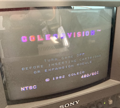
- No game cartridge, which is okay because the BIOS will go to a screen saying “please turn off and insert a cartridge;”
I plugged it in on my bench without being connected to a TV, and checked for good voltages and clocks.
My diagnosis proceeded:
- The sound chip had 4.98V across it. However, the clock pin didn’t seem to be pulsing.
- The TMS9918 VDP’s clock pins reported a steady 10.743MHz, which is 0.4% off the mark as opposed to the stated tolerance of 10.738635MHz +/- 0.005%. That seems like a big difference. Did I pick the wrong load capacitors for the crystal?
- Regardless of whether it could reliably generate video, something was happening on the VDP, VRAM, and support chips - multiple lines were being pulsed. Good enough for now, we’ll worry about the video output later.
- Nothing happening at the BIOS ROM or the RAM.
- Nothing at all seemed to be happening at the CPU, even the clock. Weird, since the 3.57MHz clock showed up on the previous boards before I split the TMS and CPU clocks into separate crystals.
- The 14MHz oscillator for the CPU was working.
- When I plugged it into the TV, I just got a white flash on the screen when the machine is powered on and off. This reminded me of how the PV-7’s dead VDP acted, but because the rest of the VDP was working I wondered if the VDP clock might be even more wrong than I thought.
Seepy You
To fix the CPU clock, I removed a couple of components that were present in the original ColecoVision clock schematic but that I probably didn’t need anymore now that the clock divider had been removed. I’m not entirely sure how they kept getting put in there, but once they were pulled, the CPU started reporting 3.57MHz on the frequency counter. Hooray!
Still, nothing was happening, so I kept probing:
- Nothing was happening on the bus;
- Nothing was happening with
/M1or the other pins that you would expect to be present for an instruction decode; /HALTwas not asserted, which is great;- However,
/WAITwas asserted. All the time.
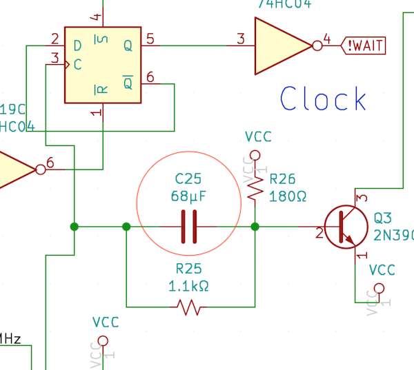
It appears I forgot to transfer an inverter from both of the original schematics into my schematic. I ended up scraping the trace off the motherboard, removing an extra pullup I had added in parallel for no reason, and then inverting the /WAIT signal using the leftover gates on one of the largely-unused 74LS05s. See, it came in handy after all!
After scratching out two traces (the trace for /WAIT exiting from the flip-flop goes in two directions, one towards the CPU and the other towards the sound chip) and then patching appropriately, I now had a correctly inverted /WAIT signal on my no-longer-pristine board. Would it be enough?
When I fired it up again, /WAIT was pulsing (probably driven by /M1) and some activity seemed to be happening on the bus. The CPU was working away diligently, although I didn’t know for sure if it was actually executing code from the BIOS ROM.
Right after this, I accidentally attached the sound chip’s clock pin to /WAIT (instead of the CPU clock, which is in the opposite corner of the Z80) and broke everything again. Flipping boards over confused me! Once I fixed that, the sound chip would issue its usual irritating “I’m uninitialized!” tone but not shut off, even though the BIOS should command it to. Something funky was going on there.
No video, either, but I was getting in the right ballpark. I decided to swap the caps on the TMS9918 crystal to try and bring its high clock rate back down to earth.
Texas (Instrumental)
Swapping the 33pF crystal load capacitors out for a pair of 56pF capacitors produced a solid 10.741MHz on the frequency counter; still not low enough (0.02% off instead of +/- 0.005%). The PVM remained incapable of sync.
Once I looked at the schematics, I remembered that I had meant to check my crystal circuit before sending the board to production. This is why:
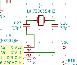
It should look like this, from the TMS9918 datasheet:
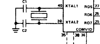
Probably what this was doing was muting or warping the clock so that it was still oscillating, but not at a level that the chip could use. This explains why the logic probe wasn’t picking the clock up on these pins. Despite all this, the colourburst clock and the /24 output clocks on the TMS9918 still looked okay.
Regardless, this should be a clean bodge. I cut away the clock traces from the VDP and fly-wired the clock pins of the VDP to the crystal. Then I fly-wired the leg of the caps to a convenient ground point nearby.
I could now see the pulse with my logic probe on XTAL2, which is good enough for me. XTAL1 just remained low, which I assumed was because of the way that the crystal works. There was still a lot of activity on the video chip’s memory bus, and the colourburst and /24 clocks were still fine.
Don’t Be An I/O Enabler
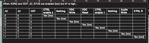
However, nothing was happening on the /CSW or /CSR or /INT pins. You usually expect to see activity on these pins when the CPU is talking to the VDP, and this was stone dead. So were the enable pins on the sound chip. It took me a while of grunting and staring until I eventually decided to check the decoders who are responsible for translating IO port and memory address requests into device chip enables. I was surprised to find that all the outputs were high! Nothing was being decoded.
I checked the schematics to try and understand if I had made a simple mistake, and I had. On the original ColecoVision, there are all these pins for external decoders. This is so that you can put in an expansion module (i.e. the ADAM) and have it “take over” the memory and I/O buses, to add more peripherals or memory. The original decoder is locked out and then someone in the expansion unit handles the decoding from now on.
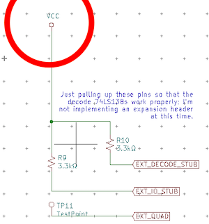
When I did it, I didn’t want to keep the expansion bus, so I added two stub pins and pulled them high, like the schematic indicated originally.
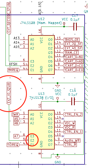
The decoders for I/O and memory decode are a little different. For memory, the expansion module has to go low on its override pin because it’s wired into E3. For I/O, the expansion module has to go high on its override pin because it’s wired into E2. I had forgotten this and pulled I/O high instead of low. This is because, as I said before, in the original schematic, it’s pulled high, but then it goes through an inverter that I forgot to include (because I saw no reason to waste an inverter gate on something that would never change.) See a pattern developing?
As you can see from the below table, pulling E2 high just turns the damn decoder off, like it was expecting me to plug an ADAM in after all.
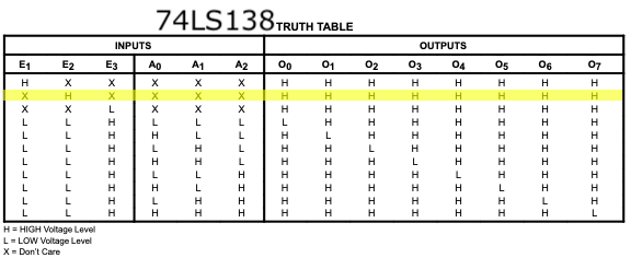
So I had completely disabled the entire I/O decoding mechanism. Lucky for me this was another easy bodge. I pulled out R9 and then patch-wired the “chip side” of it to a nearby ground pin. Now E2 would always be low, and the chip would actually function properly. A quick check with the logic probe confirmed it, but I was hardly ever seeing an /IORQ signal. In theory, I should be getting I/O requests all the time (first to shut up the sound chip, and then to write to the VDP) if everything is working properly.
Command Structure
Maybe the CPU was just executing random line noise and not the BIOS ROM at all. Let’s take a look and make sure that both /CE and /OE are active on the BIOS ROM. Both of them were active, but not necessarily at the same time. On the logic probe, /OE produced a sort of delightful twinkling music and /CE produced a harsh klaxon-y sound. If they were being activated at the same time, they should have the same tones, I figured.
After looking at the schematic a little while longer, I shrugged and then cut A11 off the /CE pin and bodged it to the /OE pin. This seems to have improved things a lot.
- The sound chip is muted on startup, which is one of the first things the BIOS does;
- Indeed, the sound chip is getting its enable pin toggled, so I/O port decoding is working;
- And the
/CEand/OEpins on the ROM are being strobed, which is what you’d expect when it’s being requested. So memory decoding is also working! - However, the VDP’s
/CSRand/CSWpins aren’t getting toggled. These come from the I/O port decoding too - which one depends on the state of/WR, but they should respond to the same range of I/O ports. /WRis getting toggled, so we should have all the conditions possible to access the VDP, but are they all happening at the same time?- I’m also noticing a bit of inconsistency. If I power off the machine and power it back on, the
/IORQline seems to behave/sound differently from run to run. Maybe something is funky with the reset circuit?
To make myself feel better, I put a cartridge into the slot to admire it.
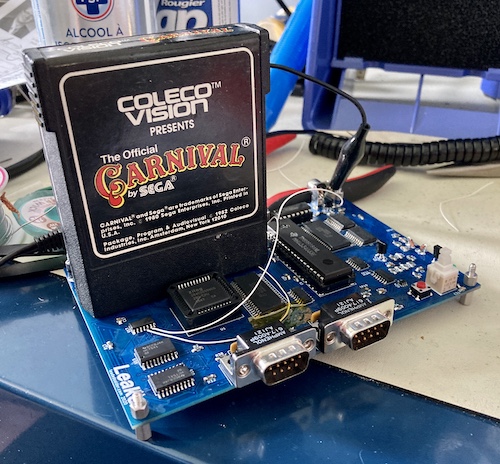
The slot definitely had a death grip, and as a result the board bent more than I would like when the cartridge is being pulled out of the machine. I wasn’t sure how to reinforce this for reliability, or if I should have just looked for a cartridge slot with a little more generous tolerance (the Sullins slot’s 1.57mm is narrower than the 1.6mm+ of the cartridge PCBs). I ended up replacing this slot with a looser one - cheaper, to boot - but look how cool it looks in the meantime!
Write To Us At Station VDP
I also found out that the guide for the ColecoVision’s I/O map appeared to be wrong; with this decoder setup there’s no way that “$40–$7f” would activate the VDP. It looked more like the BIOS ROM was writing to $BE (data port) and $BF (register port,) which satisfies the decoder by setting A5 and A7 high but setting A6 low. That address line configuration covers the range $A0 – $BF.
So I’m pretty sure my decoder logic is good, which makes sense as it agrees with the two schematics I have access to, and also the official Coleco ADAM schematics - which include a modified version of the original CV board as the “Delta” PCB.
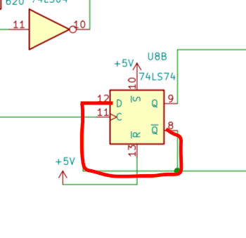
Work RAM Output Enable Is No Laughing Matter
After thinking for awhile, I decided to just go over everything I’d modified from the original schematic. Eventually I came across this little circuit, which you may recall I was proud of in the previous entry:
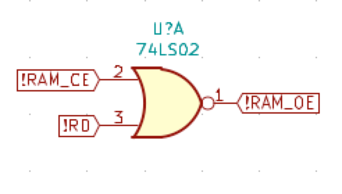
I didn’t do this right. What I was looking for is “when /RAM_CE and /RD are low, /RAM_OE should be low.” A 74LS02 is a NOR gate, and a NOR gate has a truth table like this:
| A | B | NOR gate output |
|---|---|---|
| L | L | H |
| L | H | L |
| H | L | L |
| H | H | L |
But what I actually wanted was this:
/RAM_CE |
/RD |
/RAM_OE |
|---|---|---|
| L | L | L |
| L | H | H |
| H | L | H |
| H | H | H |
So exactly the opposite of what I built in that circuit. This means that the Leako could write to memory, but never read from it. Yes, that seems like it might cause some problems…
I didn’t think this through properly because I was still in “software thinking” (boolean 1 = “on”). That’s my excuse. Anyway, I still had some leftover inverter gates…
I cut the /RAM_OE trace from the NOR gate, and wired it into an unused 74LS05 inverter gate on the top side and then back into the RAM. Testing showed that only low signals got through to the RAM, which is I guess why you buy an “open-collector” 74LS05 instead of a regular old 74LS04 inverter. Learning the hard way: that’s what I do.
After adding a 1kΩ pullup with another bodge wire so that “high” signals would show up on the pin again, it appeared that the /RAM_OE line was working. Of course, the BIOS never reads from system RAM when it’s doing the initialization, but we’ll probably need to be able to read from RAM in order to play videogames.
Of course, right afterward I was pointed to the datasheet for the Sanyo SRAM. It turns out it’s actually pseudo-static RAM, which decays if it’s not constantly refreshed. We need to hit the /LOE/RFSH pin on the main work RAM more often than just a RAM output enable would. I tied in the /RFSH signal from the CPU (how handy, thanks Zilog!) which was already inverted elsewhere on the board, and routed it through a NOR gate so that the main PSRAM would be refreshed even when it wasn’t being read from. This ended up undoing part of my bodge in the previous step:
RAM_CE |
RFSH |
NOR |
|---|---|---|
| L | L | H |
| L | H | L |
| H | L | L |
| H | H | L |
And then I just wired the output from that NOR into /LOE/RFSH on the work RAM.
Now, at least, I can cross off “values stored in RAM spontaneously decay” from my list of things keeping me up at night.
When testing this fix, I also noticed that /VDC_W pulses once at system reset and at cold start. Either I didn’t notice this before, or one of the other changes made it start working again. This means that at least the decoder is talking to it. However, I assume that the CPU should be pulsing it a couple times after boot in order to upload the text and ColecoVision logo for the startup screen… so something is still not right.
Stop Trying To Make Sync Happen
Remember up above, where I screwed up the footprint for the main power FET? Surely, I wouldn’t make the same mistake with the many through-hole transistors on the board.
I finally dug out the Tektronix 2246 scope that I have and started scoping everything on the board. A lot of things were screwed up on the TMS9918 - output signals, output clocks, input clocks, and even data pins! It looked fine on the logic probe! After an hour of freaking out and even swapping the TMS9918 out for another, I realized that the “tombstoned” clock capacitor bodge had come undone on one side and was just randomly floating around the board instead of being firmly attached to ground. That’d do it.
Now, everything looked okay on the scope - except composite output. That looked like a smeary flat line with a bunch of garbage on it at the jack, and sort of like very low-powered composite video at the chip leg. Something was wrong with my video amplification circuit, which I think I cribbed from one PDF or another.
After several more hours of probing things with the oscilloscope and being held by the hand, a patient friend, Chartreuse, consulted the schematic and then pointed out that my pinout for the 2n4401 transistor I was using for the composite output was wrong. I immediately bodged it, and added a 220µF capacitor for good measure:
Check the scope:
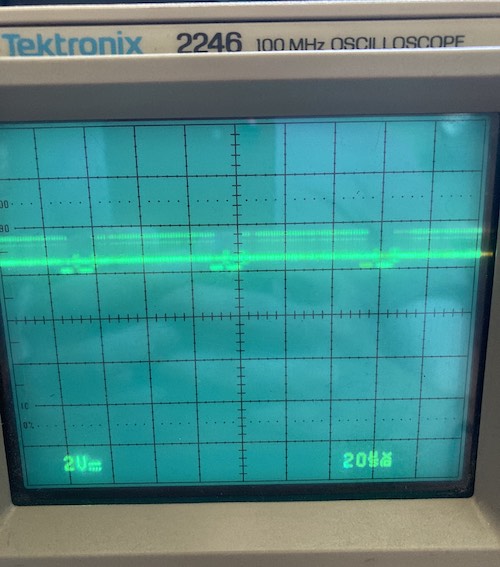
Now it looks like composite video ought to. Will it work on the TV?
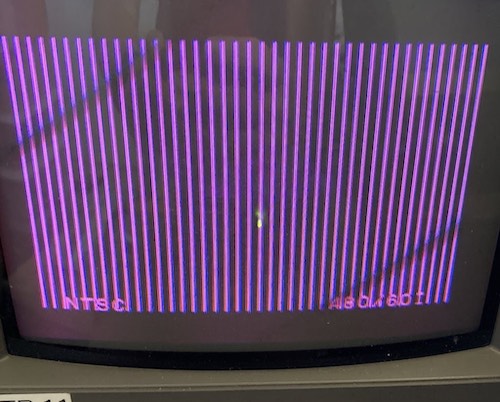
Working sync! The video itself is all screwed up, but we have video output!
I noticed that I could interfere with the video by waving my hand on the right side of the board, and whenever I touched the VRAM chip it got much worse. After touching up the ugly-looking solder joints on the VRAM chip, it became much more consistent. I should’ve left more room for myself to drag solder, or at least put the VRAM on before the VDP socket.
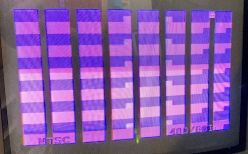
I started to see something more interesting. It’s still not anywhere close to the right picture, but it made me feel better that it at least was solid.
Everyone was a little flummoxed by this. It certainly seemed like the VRAM was not being addressed or used properly. The Sanyo datasheet was more than a little ambiguous, and the source (Alibaba chip scrapyards) somewhat suspect, so it was determined to try and get a more-understandable 62256 static RAM chip in there.
At first, I tried to bodge-wire all 28 lines onto the existing RAM chip, but I ran into a lot of trouble. Every time I’d touch one pin to adhere a bodge wire, two or three adjacent ones would pop off from the reflected heat. It was very frustrating, so much so that I just decided to order another board.
I wanted to replace the Sanyo PSRAM with a more common SRAM for awhile, because other people had expressed interest in building their own, but “ordering more salvaged Sanyo PSRAM from China” is not a sustainable part source. My contact over there pretty much intimated that even getting the ten chips I did get was a bit of a Herculean effort, and it was way more expensive than just buying off-the-shelf 62256 SRAM. To further ease assembly and trace routing, I also changed it to through-hole 62256.
For some reason, not all “62256” SRAM has the same pinout. I had some Cypress stuff in my pile, but it had a different pinout than the Alliance Memory AS6C62256 that I ended up picking up from Digi-Key. I figured the faster speed (55ns vs. 120ns) wouldn’t hurt either.
After spending a few hours re-routing the work RAM and video RAM traces, I sent away for a v0.6 board. I was feeling really good about this one!
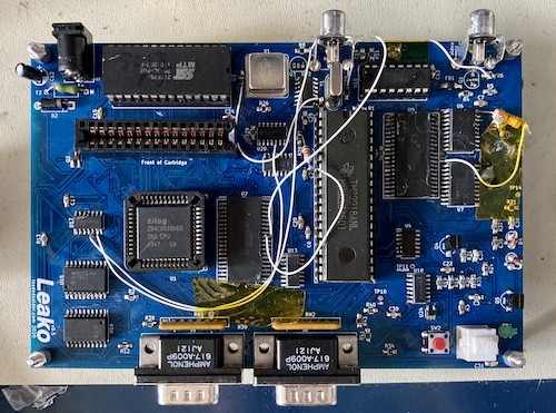
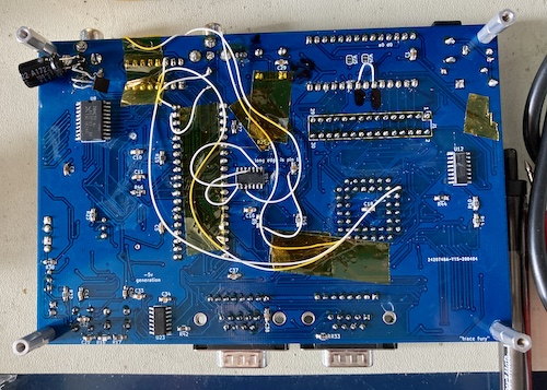
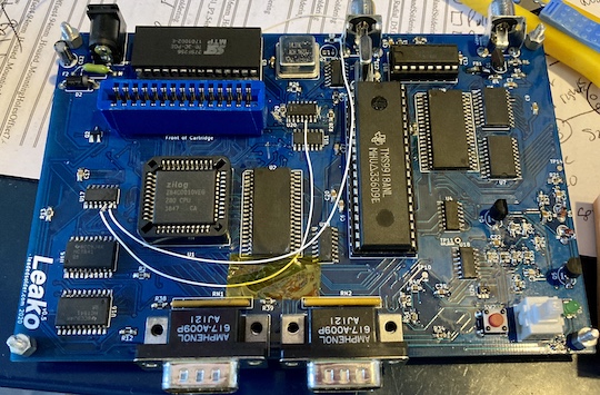
Before it goes, let’s appreciate the sheer number of bodge wires this board had. Now we know there’s some mad science going on.
v0.6
I really wanted to make it work with the previous board, but at some point it’s easier just to copy down all your existing bodges and go make a new board.
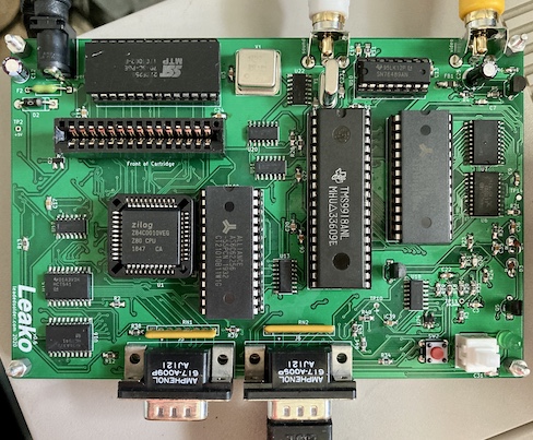
After a relatively short assembly time (~3h), I was ready to test the board again. And I got something that looked like we were in the neighbourhood:
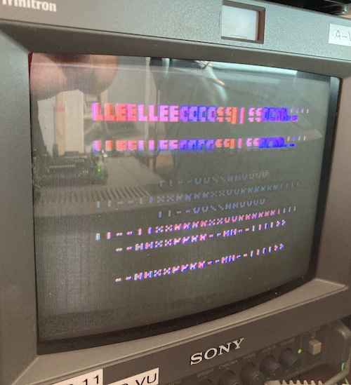
You can clearly see parts of the “ColecoVision” logo, as well as some ASCII text. With a controller plugged in, I could even proceed to the “Skill Select” screen and past it to start a game.
I tried firing up a game (Zaxxon) and it worked great - corrupted video and no ability to move the spaceship, but I was able to trot along, crash into a wall and get the death sound. Timing seemed right.
Carnival played the music I expected (see video above.) As far as I could tell, the system worked but not the video RAM. The “tiles” were all corrupt.
When I pulled the board off the TV and looked at it, there was an obvious bridge on two pins of one of the flipflops that went into the video RAM. I don’t know how I missed this during assembly, but with flux and a swipe of the iron it was a pretty easy job to clean up. I plugged it back in, and…
Holy crap.
Carrot and the Stick
Games seemed to load and run fine. Donkey Kong worked and played its great little music, and decremented lives when Mario got wasted by a barrel.
Unfortunately, the joystick and fire buttons didn’t work - just the numpad. What was wrong here? I figured it could either be my salvaged joystick or the flipflop that is intended to switch “modes” on the Coleco controller when polling it.
When I put a known-good joystick into the left port, it behaved the same as before. At least I know it’s my fault now… for kicks, I tried swapping the rescued joystick into the right (“Player 2”) port and fired up the machine. Now Mario would move to the right and jump when the button was pressed, but he wouldn’t do it smoothly - only in stuttery fits and starts, like the console was only “listening” to the controller occasionally. To make matters worse, the numeric keypad was also moving him around, which tells me that both the player 1/2 and “mode” switching was not working properly.
That said, with some tricky timing around the periodic lags, I was still occasionally able to make Mario hop over a barrel, which brought back some good memories. The next barrel would completely ruin his day, however.
That’s a good enough place to stop for now as this entry has taken forever - in the next part, I’ll work to get the controller logic correct and then start tuning the video output and try out more games.
I’m really happy to have gotten this far with the project so far. It’s definitely the biggest old-computer project I’ve ever worked on, and I’ve learned a ton from jumping in at the deep end.