Adding composite video to a Famicom
Tags: console nintendo famicom mod homemade-hardware
Since I’ve been reading I Am Error, I’ve been getting more and more interested in the technical aspects of the Famicom. Turns out all you really need to get me interested in your console is prose explanations of how a pattern table works. Also, I get to drip some molten lead into it so I can use a modern TV! Everyone wins.
When I was growing up, a lot of my friends had an NES, but I first had the ColecoVision and then a “Model 2” Sega Genesis when that came out. As a result, I’ve gone the last few decades thinking the NES was full of branded shovelware, because it turns out that’s the exact kind of game that eight year old boys bought a lot of and then subjected their friends to.
Later, when I was getting interested in collecting old videogames, the NES had already started its stratospheric price rise for many games, and with it came the skeeziest members of the game-price-speculator community. None of the cool modern “community” stuff existed then (NESRGB, Everdrives, FDSStick) so I gave the entire system a wide berth and decided to wait until this whole fad was over and prices returned to normal. That hasn’t happened yet… however, in Japan, stuff is still really cheap due to the massive popularity of the Famicom, and the Famicom is different enough from the NES that I’m coming at it without the same preconceptions that I had of those childhood NESes.
Out of the box, the original Famicom only has RF output. If you’re not familiar, this video by Gravis is the best I’ve seen on how RF output works, and a Nintendo is even used to make it relevant to this post.
Not only does the Famicom only have RF output, the Japanese channel frequencies are such that that RF output only appears on channel 95 and 96 on a Western TV, which a lot of TVs simply can’t reach. On some models, you can tweak the pots on the RF can to bring that down to US channel 6 to get around this. However, I wanted to play my games on a Commodore 1702 or a PVM, neither of which have an antenna tuner of any kind. Doing a composite mod seemed like the easiest way forward.
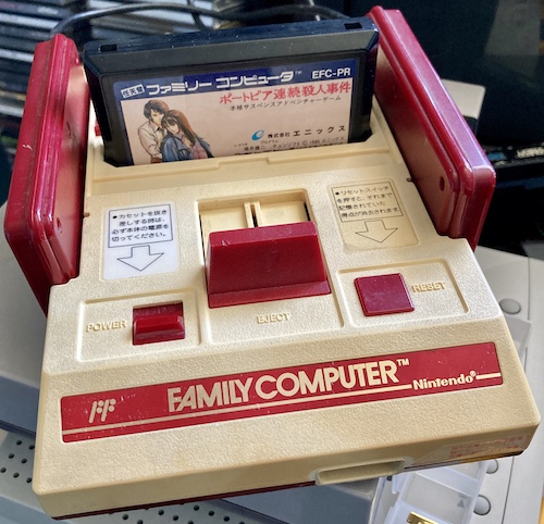
Giving It A Good Squint
The first thing I noticed is that a Famicom is a lot smaller than an NES. They added a bunch of empty space for the American model in order to accommodate the “toaster” mechanism, I guess.
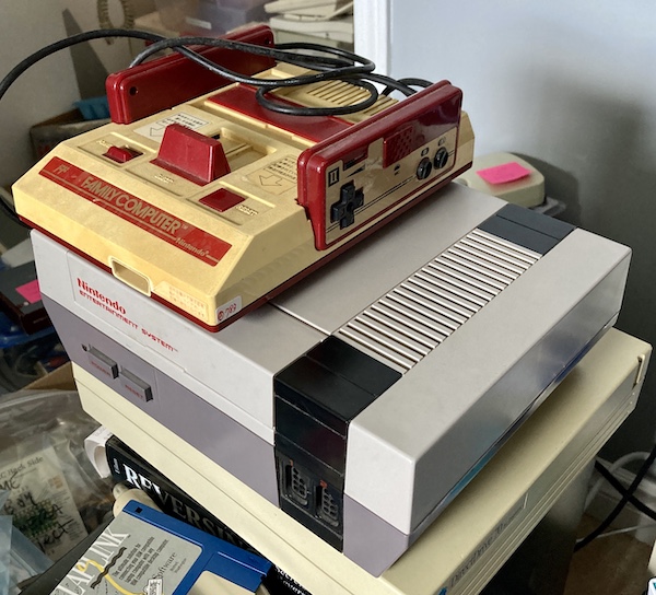
I thought I would hate the hard-wired controllers, but they’re actually really nice. You’re guaranteed to always get first-party controllers when you buy a used system, which is more than I can say for basically any other machine, that NES included. It would be nice if they were in better condition, but if they work I’ll be happy.
There’s a “Famicom Family” logo on the front sticker that I haven’t seen on most other Famicoms; from what I can tell, this is a good way to tell what machines are later models as it ties into some kind of later branding.
Opening It Up
When mine arrived from Japan, it looked dirty and pretty beaten up, but that’s okay for a test machine. I can always get a nicer one later; another thing to hoard.
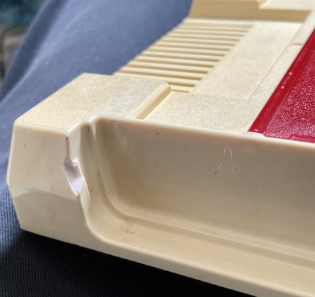
A corner of the plastic near the player-1 controller mount was missing, and there was grit in the textured plastic. I took a few trips to the sink with the plastic and scrubbed, but the yellowing is obviously not going to come out with soap and water.
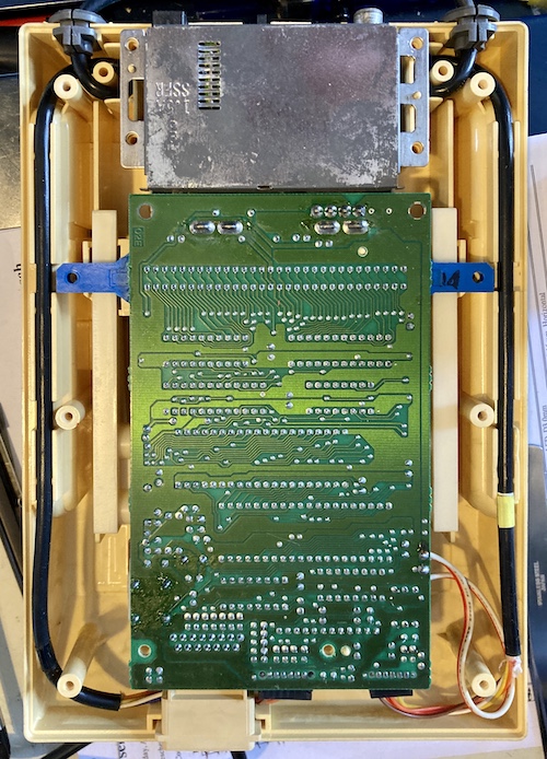
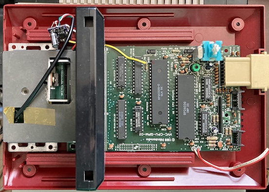
I opened it up - screws were tight, a good sign - and then took a look at the board. It’s a late model, as evidenced by the big power/RF module soldered to the board instead of attached by a ribbon cable.
This console has spent some time in an old shed or something, based on how much of Mother Nature had crept inside of it, but at least I didn’t find any stray cigarettes inside it unlike the above NES. The motherboard cleaned up quickly with some spray alcohol and cotton swabs.
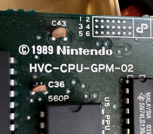
The board is a 1989, which was a pretty good year for Nintendo. The Famicom apparently kept getting made until 2003. It would be cool to track one of those down.
I wanted to deep-clean the dirty, scratched-up controllers as well - the controllers still had their protective plastic wrap on them, but they were scratched anyway! - and make sure that the silicone on the D-pads were in good shape, but I stripped one of the screws on controller 1 pretty severely in a moment of clumsiness. I’ll drill that out later and service it, but in the meantime let’s get back to the composite mod.
Motherboard Work
I got sort of lucky in having a late-model board. On the later boards there’s a dedicated “video” pin that is broken out near the RF jack that I could just solder to, rather than lifting pin 21 (VOUT) of the PPU. This way, you can keep both the RF and composite. Reportedly, this creates a bunch of ‘jailbar’ interference, so I’ve done what others have and lifted pin 21 of the PPU. Sometimes the hard way is the best way.
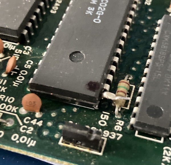
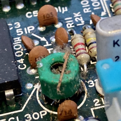
This wasn’t too hard to desolder and lift, but the pin would have looked a lot less mangled if I had also desoldered R6 first to get it out of the way. I had to use a little bit too much force on my “prying tweezers” to lift it out, which could have easily broken the leg on a newer chip where the legs are much more fragile. Thanks, 80s technology!
I also added decoupling caps between 5V and GND on the CPU and PPU chips. It’s just good practice! These 0.1µF axial ceramic cuties were lying in my cap pile ever since I used a handful of them for the cursed Tandy 1000SX, so I was happy to slam two more of them in. The recipe I was following used /RESET as the 5V source, which feels a little sketchy, but it means you don’t have to run long wires all the way to the other end of the chip. Then again, the copper pour on the back of the board is 5V…
I thought 0.1µF might be a little small, but it’s easy to change these out for a 1µF or larger cap if it doesn’t have much effect. You probably shouldn’t pick decoupling caps based on aesthetics.
Video Amplification
The whole idea behind the composite mod is that you’re building a simple signal amplifier to replace the one that was originally inside the RF can.
As the baseband video signal comes out of PPU pin 21, you need to step it up to a level that the TV can easily understand. The video chip’s output transistors are simply not designed to directly drive a television, and after the weak signal goes all the way through the AV cable into the back of the TV, there’s probably not much left to pick up anyway.
There are a lot of homebrew mods for this, ranging from cutting out and reusing the stock transistors on the motherboard to building a whole protoboard circuit with some new parts.
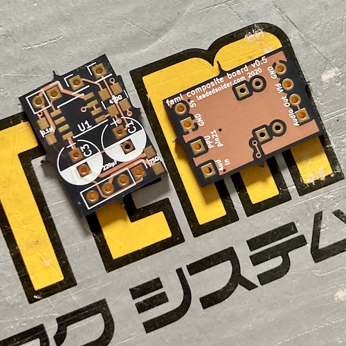
After doing some more research, I decided I would try a part that I’ve been meaning to try for a while, the TI THS7314 video amplifier IC. It’s used a lot for the amplification of analogue RGB signals, and it should work really well for my one-channel signal. The part is designed specifically for this application, and should both install cleanly and produce nice-looking video.
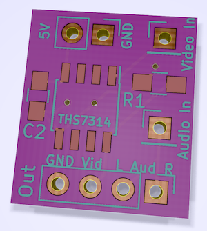
I made a quick, super-simple little board that basically just broke out the pins of the video amp chip, and sent it to fab at OSH Park. They’ve recently added free (if slow - over a month) shipping to Canada, which makes them a really desirable option for running off onesy-twosie little mod boards like this during the current shipping nightmare we find ourselves in.
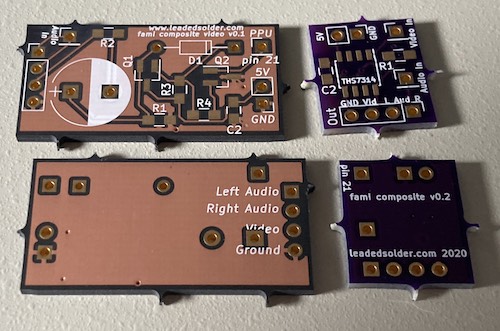
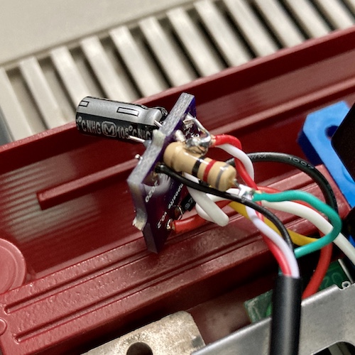
I made boards to do two variants, one with the original “homebrew” amplifier circuit and one with the THS7314. If the THS7314 doesn’t work out for whatever reason, I can just put in the usual circuit that the community prefers. However - spoilers - the THS7314 worked fine, so I never actually constructed the traditional design.
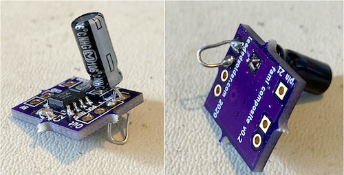
I should have added a jumper to the board to solder left and right audio together (the Famicom is monoaural.) This ugly cap leg trick should be fine for awhile. I decided on a 220µF capacitor for audio, because that’s what was on the top of the cap bin when I opened it.
Sound
The Famicom supports audio coming from the cartridge, which is why Castlevania III on the Famicom has such better music than that on the NES. I definitely want to be able to hear the cartridge audio, so it’s worth pulling the audio from somewhere other than directly out of the CPU (which also contains the sound hardware – lower chip counts = more profit for Nintendo.) The “audio output” pin on the cartridge contains the Famicom’s sound after it has been mixed between the expansion audio and the system audio, where it normally then travels immediately to the RF can for output. Since we’re no longer putting that audio into the RF output stream, it needs to get broken out and fed into the TV using the usual RCA jacks as well.
Reportedly, the GPM-02 motherboard has a different ‘mix’ between the expansion audio and the system audio compared to the original Famicom motherboard. You can revert back to the original model’s amplifier behaviour by removing the 43kΩ resistor at R7 and replacing it with a 100kΩ part.
I also removed the choke at FC1 on the motherboard, so that the sound didn’t go into the RF can where it might pick up other noise. To source audio, I just went from the “expansion audio” pin (#46) on the cartridge port and added a 220µF capacitor.
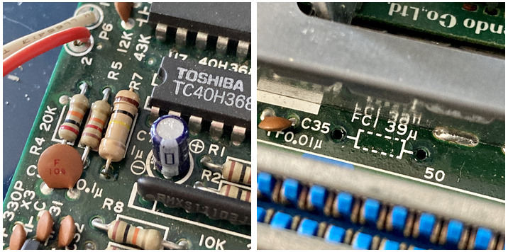
I only had a giant 100kΩ resistor on hand, so that’s the one that went in. This bugs me more than I thought it would.
These changes seem to make a pretty significant impact. I generally don’t have an ear for little tweaks, but this is big enough that even I can pick it out. There’s whole instruments that seem to be missing from the unmodified mix.
Getting The Signal Out
There’s a lot of different ways I’ve seen of actually getting the composite signal out of the Famicom and into a way that you can plug it into a TV:
- Cut out the RF box’s antenna jack, and replace it with a TRRS jack, which carries all four signals for RCA on one jack;
- Drill holes in the side and put in some panel-mount RCA connectors;
- Run a female or male RCA cable squid out of the case (usually through the player-two controller grommet);
- Replace the entire power and RF board with a board of your own design;
- Or some combination of the above. There’s no real “best” way established for doing this, which makes the mod more interesting in my mind. Each machine has a bit of its creator’s personality.
The way I wanted to do it was to put a TRRS jack inside the top RF box, replacing the antenna jack entirely. However, the antenna jack is soldered into the shielding of the RF/power unit:
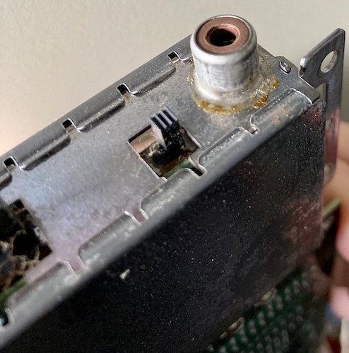
I thought about attempting to desolder it, but the RF shield is likely to sink a lot of heat and damage the other components nearby. On the ctrl-alt-Rees guide, he cut out the RF shield around this jack using a hacksaw and then desoldered the jack from the motherboard, which left an obvious square hole in the shield, but looked good from the outside once the case was reinstalled. That works for me, especially since the RF jack became useless as soon as the PPU’s pin 21 was lifted. The plan was for the TV/Game and CH1/CH2 switches to stay for now, although maybe they’d be useful for some other cool mod later.
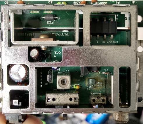
I made sure to check the fuse here, as I hadn’t actually run the machine at this point. Some of these solder joints are pretty gross.
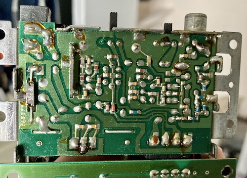
The top and bottom plates of the RF “box” can be popped off with a flathead screwdriver, and I decided to take a look around to see what the engineering was like. It is about what I expected, but I had hoped for more empty room in here for stuffing in mod boards.
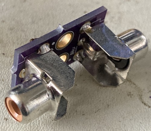
Finally, I decided on removing the RF jack and replacing it with a TRRS jack. I grabbed a TRRS video/audio cable and a “Gikfun” breakout board off Amazon, because they were available on Prime shipping and the whole theme of this project is apparently that I am feeling very impatient.
Then I started removing butchering the RF jack. I got a pair of tin snips, but they were too big. I ended up using a pair of pliers and my sacrificial side cutters. This did a pretty decent - if slow - job, up until I accidentally broke the end off the TV/GAME switch.
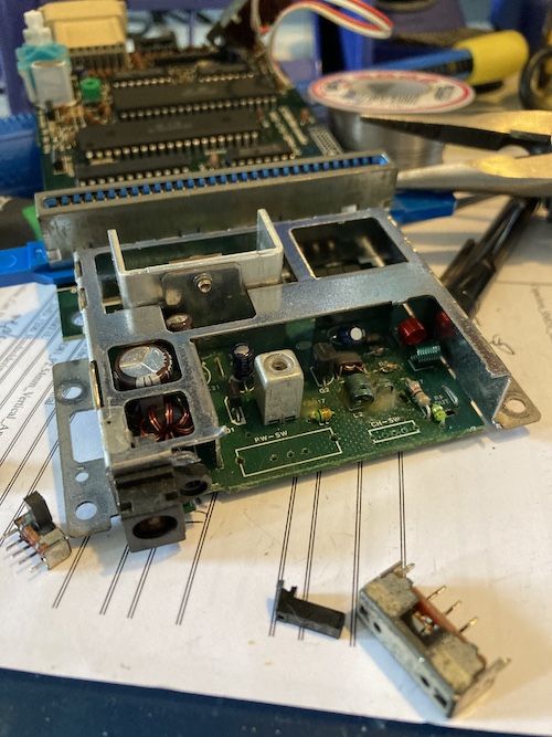
After that, I decided to desolder the two switches and cut all the back shielding off. The result didn’t look great, but I was able to file back the sharp corners and then remove the components near the former place of the RF jack so I could fit the TRRS breakout board in.
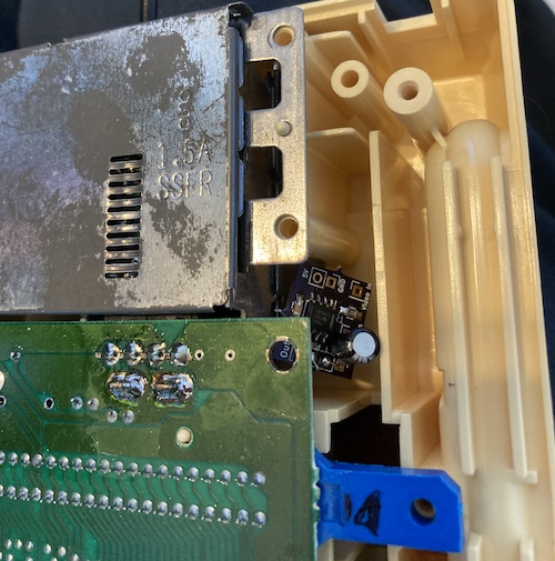
Unfortunately, I couldn’t figure out a way to mount the breakout board. I tried with two-sided tape, zipties, and even soldering in a retaining wire and found nothing would really work that well. I considered two-part epoxy or a 3D-printed thing that I could rivet onto what’s left of the RF shield, but until I know that the mod works it’s probably not worth doing anything permanent yet. I ended up grabbing another TRRS pigtail off Amazon, this one female, and then routing it out the hole in the back of the case. Yes, it’s ugly - but it works.
A bit of trouble arose when I was figuring out a good place to mount the board, as well. I didn’t want the TRRS pigtail cable to interfere with cartridge insertion, but the bottom case left me very few options.
I ended up cramming it awkwardly next to the RF box, and using two-sided tape to insulate the solder joints from the RF shield. It would have been nice to make the AV mod board just a little bit bigger and have a mounting hole, so that I could at least zip-tie it to this unused screw hole on the motherboard. If this were an earlier-model Famicom, I definitely think the right thing to do would be to completely delete the RF/power board and fabricate my own, but for now we’ll just limp along with this awkward setup. My soldering iron doesn’t have enough oomph to completely desolder the RF board from this machine.
TRRS Fun
There were a few difficulties with using the TRRS jack for AV output. Apparently, there is no actual standard for the pinout on a TRRS jack that carries composite video and stereo TV audio. I decided that I would just use the pinout from whatever cable I could get from Amazon, and when it arrived I buzzed it out to determine the pinout.
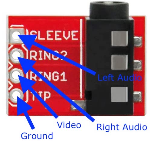
Mine ended up looking like this, but your cable is likely to be different because we live in an imperfect world full of people who refuse to adopt a consistent pinout. On the Raspberry Pi, for instance, the video and ground signals are flipped, so this cable wouldn’t work.
As mentioned in the previous section, I didn’t end up using the pictured TRRS breakout board because it was too difficult to mount securely inside the wreckage of the RF box, but it’s still a good pictoral explainer of the pinout of my specific TRRS AV cable.
A First Test
I had a lot of trouble trying to get the mod board and all the wires attached into a good spot in the case, so for the initial testing I just ran it sitting outside of the machine. You might think there is a lot of empty room in here, but it goes away very quickly when the controller cables are installed.
Unfortunately, it seems as if the video quality is not what I had hoped. For one thing, it’s way too bright, and there’s still visible vertical “jailbars” on the output! When I turn the machine off, there’s also a white ‘flash’ that is reminiscent of when I had the Leako’s video output transistor wired up wrong. At least the audio sounds really good.
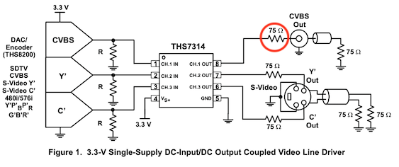
After consulting the datasheet, I saw that there’s this 75Ω output resistor. Duh, I missed a component for “darkening up” the output! After all, the example circuit had one for composite video output (it turns out the C in “CVBS” stands for something…)
I didn’t have a 75Ω through-hole resistor on hand for some reason, so I substituted an 82Ω part from a kit of 1/2W resistors. It looks a little stupid on the PCB, but the results speak for themselves:
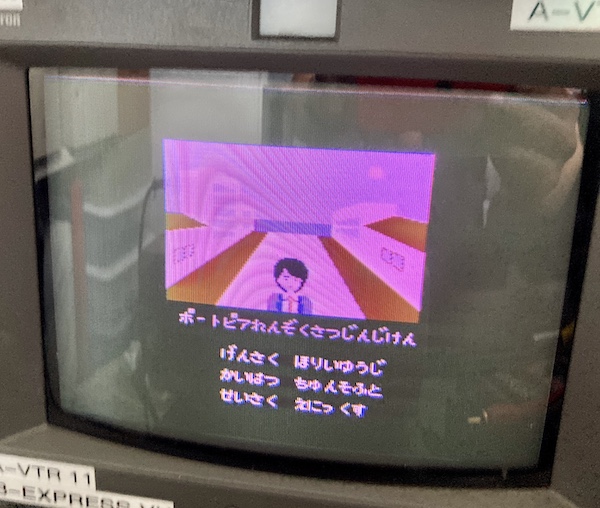
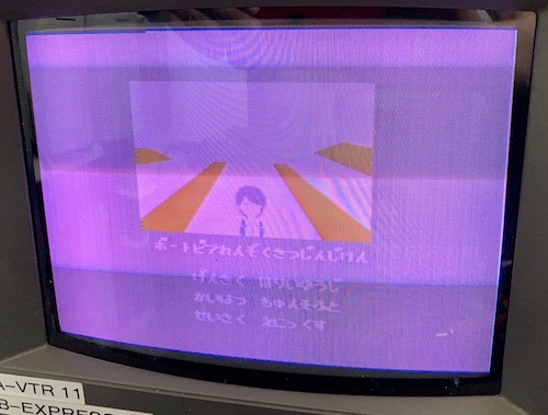
Other than the slight pink tinge of my PVM, this looks about as I’d expect it. And the white flash on power-off is almost entirely gone, too! Sorry for giving you the old spicy baseband.
An annoying problem I noticed on this early board is a bit of “flagging” at the top left corner in Hatris (which might be affecting the automatic brightness, etc on my cheap USB composite capture device as well.) A couple of the other games I own (e.g. After Burner) also have problems trying to establish “white levels” from “black levels” and look washed out as a result, but most of the games I tested seem to work pretty well. I resolved to spend a little more time testing before updating the PCB.
In other words, screw it, I’m gonna play Mario and not properly learn what AC coupling is for awhile. It works!
Make It Fit
Now it was back to my least favourite task: sticking this damn thing inside the case. You wouldn’t think it would be so hard, and yet it is. Nintendo really designed the plastics on this thing to have very little free room, likely both to ease assembly and to give the machine a feeling of structural solidity.
Not to mention that all the bodges I’ve got hanging off the back make it much more difficult to find room for:
It’s ugly, but it should work for now. I want to do a test fit at this point, in order to figure out where inside the case I should place this such that it will be okay with the case and the eject mechanism, without interfering with the cart slot.
Running any wires north-to-south on the board is tricky because of the cart slot; the blue plastic ‘tabs’ on either side are a major structural element that is securely captured by the bottom plastic with little free space, and if you go over top of it you end up running your wires through the cartridge slot, which is both ugly and runs the risk of a weirdly-shaped cartridge not being able to be inserted.
Afrer a bunch of trial and error, I ended up cramming the board into the “player 2” side of the RF modulator instead of the side pictured above, and putting some kapton tape on the metal shield of that modulator, so the joints on the board wouldn’t short to ground if something horrible happens. The eject lever’s “arms” come very close to the yellow composite wire like this, but it still has about a centimeter of clearance.
The front of the case has boatloads of empty space by comparison; if I were thinking more logically in the first place, I would have run the TRRS cable all the way back instead of the individual wires, and mounted the board in the front of the Famicom, where I’d have tons of room to do whatever I want. I think any future version of the board will have to be larger, so I will plan on putting it here instead of alongside the RF can.
Coupling’s Hard
Even though the v0.2 board worked, and the output video was legible, pretty much every game was too bright, and the “flagging” at the corner of Hatris’s boot screen worried me a little bit that sync wasn’t working properly. Adding a capacitor to the output - I tried first 220µF and then a 470µF, but they were pretty much identical - the flagging and dot crawl was reduced but not completely. The colours were still way too washed out.
After asking a lot of really smart people, the consensus was that I likely had a sync clamping issue.
I had a lot of trouble trying to understand the concepts of sync tips. It’s probably because I’m not super comfortable with AC in general. I could probably have shortcut a lot of this guessing just by hooking up my scope, but I was very limited on desk space during this project and also feeling too lazy to break it out for such an “easy” thing.
It took me awhile of fumbling, but blog friend Curt J. Sampson pointed me towards the Wikipedia page on composite video, which contained this great diagram of how composite video establishes the white and black levels:

It’s impressive that all of this stuff was figured out in the ’40s and ’50s - composite video has been very successful even if the quality isn’t the best. The designers probably would be really mad if they knew I was still trying to use it now, but in my defence a Famicom is only about 40 years newer.
The datasheet for the THS7314 mentioned that it would not operate properly if the reference levels were very small or negative, which could explain the white flash when the Famicom gets shut off. In my intuitive understanding, the TV is “getting used to” a very low black level, and then when the Famicom switches off, it has to scramble to re-adjust, sort of like when you walk outside into the daylight after spending awhile in a dark room. At least that was my guess.
I tried a whole bunch of things:
- A 3MΩ pullup on the input signal to try and force it into a range that the amplifier would like;
- A pulldown on the output signal to see if I could bring the “top” down;
- Different values of bypass caps to try and trick the chip into different “modes;”
Nothing really changed:
Ultimately, it seemed that the peak-to-peak voltage (Vpp) of the signal coming off the PPU was just too hot. 2Vpp at a 0.7V DC offset! That’d do it. I could definitely have saved a lot of time just cleaning off my workbench and setting up the Tek 2246.
Adding a two-resistor voltage divider (two 470Ω resistors) to halve the input voltage, and then dead bugging it off the PPU, seemed to get the video back in range.
Changing the 82Ω output resistor back to a 75Ω fixed most of the brightness.
Blue was still coming in bright for some reason, but the rest of the colours were starting to look correct. Everything was at least playable now, which was a huge improvement.
While testing, the power switch wires broke off the board. I guess that’s what happens when you leave them dangling loose under their own weight for several days. For a few seconds I was convinced I had somehow shorted the dead-bug mess and killed the power supply fuse. Once the wires were stripped back to expose some fresh wire and then re-soldered, everything worked okay again.
Take The Win
At first, I was going to spin a new board, but then I started actually using it to play games… and it’s not that bad! Even though the colours aren’t quite right, this is perfectly acceptable in my mind for a “first version,” and satisfied my requirement of being able to play Famicom games on a composite TV.
I think the following things should be done on the next version of the board, which I’m starting soon:
- Try picking different values for the resistors in the voltage divider. Maybe halving it isn’t the best idea and I should pick something like 1000Ω/(1000Ω+470Ω) to get 0.62 in order to pre-compensate for the drop in DC offset.
- Try using a THS7316; it’s similar to the THS7314 but without the low-pass filter that can make some signals look muddy. Not like I can tell on this tiny PVM…
- Add some attenuation resistors to the sound output. It’s extremely loud, as you can hear for yourself from all the clipping on the test videos. Much louder than a “real” NES.
- Test it in an oscilloscope using 240p Test Suite, comparing the output to an American NES or a Twin Famicom in order to verify that the colours are “authentic.” Eyeballing games on a broken TV is not science!
I’ve already built an oscilloscope “pass-through” board in order to test it, but you’ll have to wait for the next entry to see exactly what my testing ends up with:
A new PCB is already on its way, to at least avoid having to dead-bug capacitors into the middle of space:
Enjoy Some Games
It’s a little amazing that I still figured out how to close the case with all this crap hanging off of it.
When I started playing it, I noticed that pushing the “B” button on controller 1 would sometimes also activate the “Start” button. I swapped it for another controller from a different Famicom in my pile (hoarding pays off every time) and that seemed to fix the problem. When I drill out the stripped screw, I guess I have more than thing to repair on that controller.
I really enjoy this little machine, and it gets a lot of use. There’s a lot more maintenance to do on it (cleaning, repairing the old “Player 1” controller, more cleaning…) but this is now a usable system.