Big Blue vs. The Tandy 1000SX
Tags: computer tandy tandy1000 tandy1000sx custom-chip-failure repair
Thanks to the incredible kindness of another Tandy nerd, I’ve gotten a replacement Light Blue chip, but will the Tandy 1000SX finally work properly? Let’s ask the four years that I spent trying to figure out what else was wrong with it.
Recap
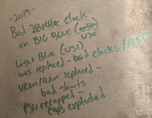
In case you haven’t been obsessively reading my past entries from 2019 (shame on you!) I bought a Tandy 1000SX a long time ago, from a flipper who had parted it out after it started sprouting RAM errors on boot. I paid way too much for it, even if it had worked perfectly when it got here.
This series of machine sports an 8088 CPU, a handful of RAM, and an interesting RGBI “Tandy” video mode as well as SN76489-adjacent sound. It fulfilled the promise that the IBM PCjr made: an inexpensive PC-compatible computer that was well suited for home use and games.
I figured it would be a challenging computer to write a game or demo for, but I ended up getting a different kind of challenge.
When the computer showed up, I immediately tried powering it on, only to get some composite video garbage and eventually a very loud bang. One of the caps in the power supply had exploded.
While repairing the power supply, I found out that a corner of the board had been broken off. That corner, unfortunately, contained a trace for voltage feedback, which was used to control the +5V regulation of the power supply. Without that trace, the power supply’s +5V rail had been allowed to float upwards, and likely fried a lot of chips as it did.
After I repaired and bench-tested the power supply, I started trying to figure out what had failed on the motherboard. Lots of RAM got white hot on startup, but I also found that there were bad reset and clock signals, keeping the CPU from running. RESET’s active-high level was being squashed down, and no clocks were coming to the CPU.
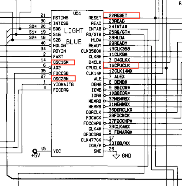
With a scope, the beyond-excellent Tandy Technical Reference Manual, and help from some smart friends, I eventually traced the failure to a custom clock-generating chip, the 8075-306 “Light Blue” at U51.
Often, a dead custom chip means the end of the machine. However, the Tandy 1000 series is popular enough, and shared enough parts between the models, that I was hopeful I could find a replacement part.
High Speed Parts Swappin’
This Light Blue came from a 1000SX parts motherboard and was kindly donated to me by an awesome member of the VCF forums, GrandPoobah, in 2019. It arrived quickly, and I plunked it in the first chance I got.
First indications were positive:
- There’s five volts at the reset switch;
- When I pushed the reset switch, the voltage observed on the pin dropped;
- The active-high
RESETpin on the CPU went high when I pushed the reset switch; - The reset signal was triggered when the machine first started up;
- The clock pin on the CPU throbbed on the logic probe.
However, I still didn’t have anything on video, and the machine didn’t seem to be doing anything. READY on the CPU was pulsing, but nothing seemed to happen on the address or data lines. In fact, all the pins on the RAM were stuck high, except for Q and RAS.
Big Blue Boohoo
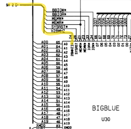
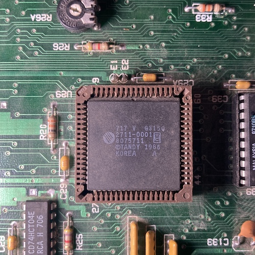
Looking at the schematics in the Reference Manual, I now began to suspect another of the Tandy custom chips. “Big Blue” at U30 is an 84-pin PLCC custom chip that controls video (not working) and RAM (also not working.) Seems like a good candidate.
The first thing I wanted to do was check its 28MHz clock input, which is located on pin 24. This master clock is divided internally by the Big Blue to provide a lot of derivative clocks for the various video- and memory-related tasks that the Big Blue handles. Just like when Light Blue was misbehaving, the 28MHz input clock seemed to be squashed low.
Page 2 of the schematics show the clock coming out of an oscillator:
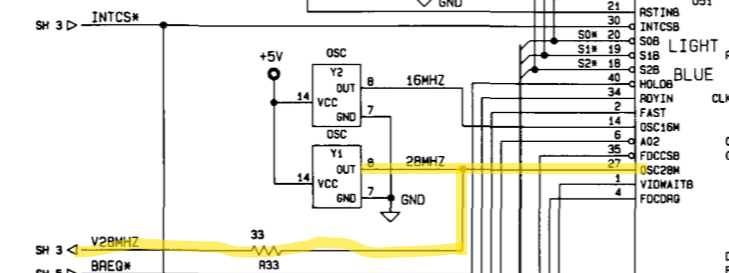
Page 3 of the schematics show the clock going into Big Blue:
The 28MHz clock comes directly from an oscillator, and then goes into both Light Blue and Big Blue. There is not much to go wrong in this circuit.
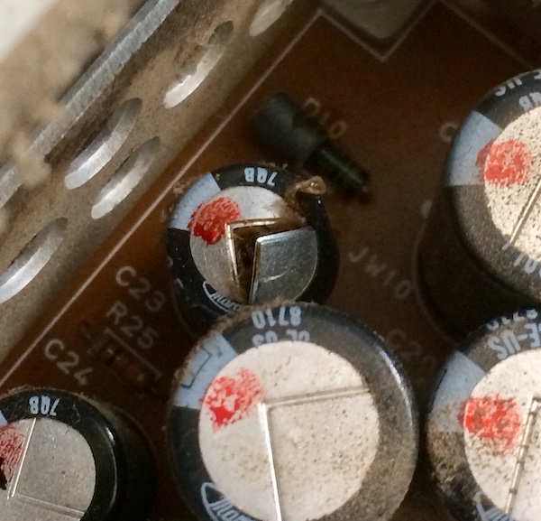
Big Blue has an inline 33Ω resistor on the clock line (the very prominent R33), so I probed for the clock on the oscillator’s side of that resistor, hoping that perhaps it was just the resistor that had blown and not another expensive custom chip. Sadly for me, the logic probe still reported no 28MHz clock.
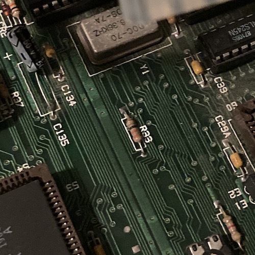
There’s some interesting shmoo on the board around R33, but it didn’t seem to be conductive, nor was it corroding a trace. Let’s move on.
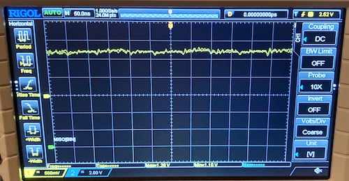
Out came my then-new-to-me Tektronix oscilloscope, to make sure that the clock was actually being squashed. The logic probe can tell you if something is working properly, but not always how something is broken. If I saw the same failure on this clock pin as I did when the Light Blue was bad, then I would be forced to believe the Big Blue had also died.
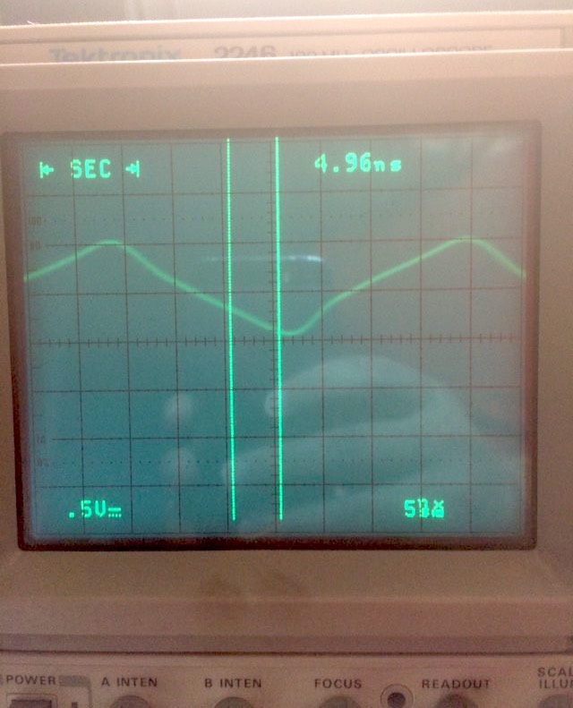
Unfortunately, the scope verified my worst fears. This failure left me in quite the predicament for this machine. At this point, I’d already sunk a ton of time and money into this 1000SX, and more custom Tandy chips weren’t growing on trees. Other broken computers arrived in my life in the interim. So I let it sit. And sit… and sit.
You can now imagine a montage of pages flying off of my wall calendar, as the years move onward from early 2019, with the 1000SX residing semi-permanently on a shelf in my basement.
In the meantime, I had purchased a Tandy 1000EX from an American estate sale, and a Tandy 1000TX from a local sketchy dude who “found it” in a basement somewhere. My plan was to use these machines to swap custom parts, and figure out what else had blown on the 1000SX. That never happened.
But then…
Big Blue Woohoo
Somehow, I had neglected to actually set up an eBay search alert for the part number of a Big Blue. In fact, I hadn’t even taken a good picture of the chip. One night, I was reading about another hobbyist’s project on the Tandy 1000, and thought of my poor stricken SX. I decided I would take a quick search, and…

Being from the US, the shipping was several times the purchase price, but at least it was going to help a charity. And I didn’t know if I’d ever see another one of these loose again.
It arrived fairly quickly, and I took the 1000SX out of mothballs to disassemble it. I was feeling a little sad at seeing it in this state again. This was one of the first repair projects I had taken on, and it always stung a little that I wasn’t able to fix it after so much time, effort, and full schematics.
Say what you will about my diagnostics, repair, and general writing skill back then, but at least I was pretty good at documenting what I tried.
I’m not sure why I put so much detail down there. Maybe I was afraid that some horrible future calamity would occur and destroy the world as we knew it in a few years? Good thing nothing like that happened, right?
With the benefit of the intervening years of experience (and many more broken systems since,) I now knew how to properly use a PLCC extractor. It still fought me, of course, but with a mighty crack, the presumed-bad Big Blue came free from the socket.
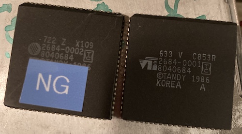
At this point, I realized that the old chip was actually a 2684-0002, not an -0001. This didn’t worry me too much, but my past experience with the computer made me jumpy to just start flipping the power switch without putting the work in.
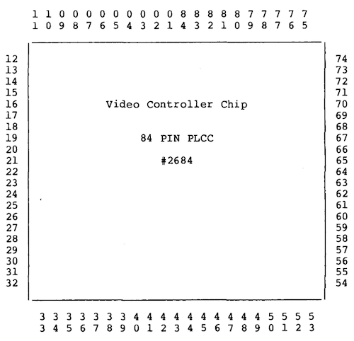
I did a little bit of research: the Technical Manual didn’t give a part number for the chip, but referred to it as “#2684” in this somewhat spartan pinout diagram. I did find out that the Big Blue seems to contain a Motorola 6845 internally, and even contains a little test ROM for it. I also asked the VCFED forums, which didn’t render up a reply within about a week, so I tried it anyway.
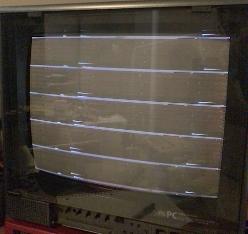
And, well, you can clearly see that there’s something on the raster here. It’s stable, too, not rolling. That’s better than what it looked like before, which was just a blank screen with no sync. But nothing happened, even after waiting for awhile.
I felt around for hot parts but found nothing except for the 8088 CPU, which was getting slightly warm.
I pulled out my newer Rigol scope (a lot easier to move around than the old 2246) and scoped a smattering of the CPU address lines. Still nothing – just a solid 1.30-ish V. Boy, that sounds familiar, doesn’t it?
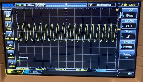
28MHz was now present (and seeming to be in the frequency neighbourhood) on both sides of R33, indicating to me that the new Big Blue was no longer pulling it down. The waveform didn’t look exactly squared-off, but I chalked that up to my scope either running out of bandwidth or me not having it in the right mode (which is more likely.)
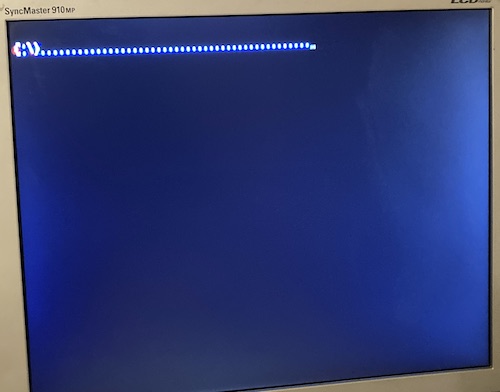
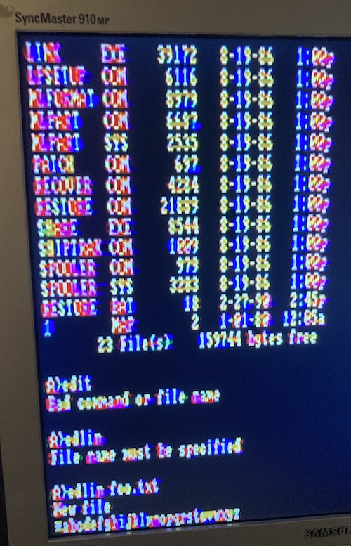
My workbench Samsung 910MP TV/monitor didn’t detect sync at all. I stuck the composite output into a BNC adapter and then directly into my scope (I couldn’t find my 75Ω terminator tee, so values on the scope will be very strong) and saw that there was indeed something that looked like a composite sync dip.
Perhaps the Samsung’s fancy digital sync circuitry was simply too picky. A dumber monitor is exactly what the doctor ordered.
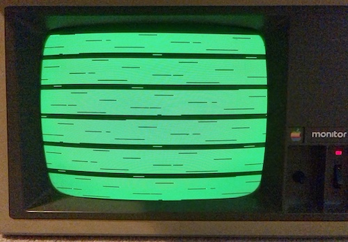
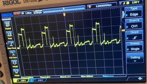
I plugged in the Apple Monitor III that I had lying around, and got a field of garbage, but oddly periodic and consistent garbage. Although it was generating something that could be perceived as video, it looked almost like the sync was wrecked, like it was out of time. This wouldn’t be unexpected if the boot process were hanging up in the middle, and would also explain the weird h-sync frequency count, since the 6845 has a ton of registers that control its specific scan rates. The CPU had simply not gotten to the point where it tells the 6845 what it’s doing, so the VDP was instead doing whatever it woke up thinking about.
See, Pee-Yew
Was it possible that the AMD-branded 8088 CPU had also died from the overvoltage event? It felt unlikely, but compared to a Tandy custom chip, finding another 8088 to swap in should be easy street.
Surprising even me, I could only think of one other 8088 system that I had on hand: the Sanyo MBC-555. And that system sports a ceramic Fujitsu 8088, a chip that I felt was too nice to risk on the 1000SX. Plus, I wasn’t sure it would come out of its dusty and rusty socket without a fight. The last thing I wanted to do was end up fixing two uncommon old PCs.
I even asked Renesas to send me a sample of their $80 space-hardened 80C88, but they politely refused, so I ended up ordering 8088s and NEC V20s from AliExpress to see which would get there first. Of course, after the eBay V20s arrived, I remembered that I also had the Tandy 1000EX. It was sitting right next to the SX in the closet. D’oh.
Pulling the old 8088 was a real fight, but it came loose from its home of several decades with some gentle persuasion. I popped one of the V20s in and started it up. A15 now seemed to be oscillating, which was a good sign.
Putting a scope on pin 20 of U41, the presumed BIOS ROM, showed that the CPU was routinely accessing the chip select on that ROM. This computer was, at long last, trying real hard to run.
This check also told me that the upper address lines were being driven for a memory access, since an 8088 CPU will start execution at $FFFF0 physical, or FFFF:0000h segmented1. The Tandy 1000SX decodes its BIOS ROM chip select within the memory range of $F0000 to $FFFFF , so at least A19 .. A16 were working.
The first instruction at $FFFF0 is an order to jump to F000:E05Bh, or $FE05B . Both of these addresses light up nearly all of the address pins below A16. The Tandy manual says that pins A12 to A15 are buffered2 by the 74LS244 at U54, so I quickly checked that (soldered down) chip in circuit to make sure that we weren’t accidentally dropping any of those lines and ending up somewhere weird, or corrupting a request somewhere down the line.
U54 didn’t make anything that looked especially bad. The ‘373 latches that handle multiplexing for the lower address pins had some gross-looking activity on the data 0 pin coming out of the CPU, and also seemed to have some oddly weak output topping out only around 4V:
I suspected that the ‘373 might be doing some fighting with something else attached to it, but there are a whole lot of other things connected to that data bus, too. I decided to stop here and check out the ROM before I went any further, mostly because I understood better how a ROM worked.
ROM: Space Fight
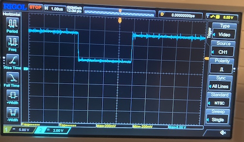
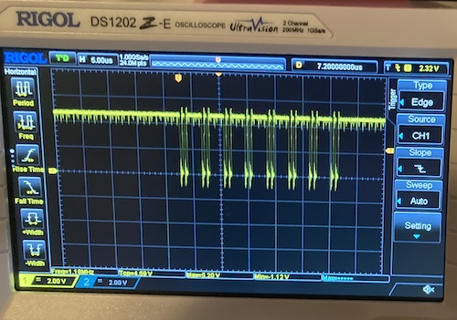
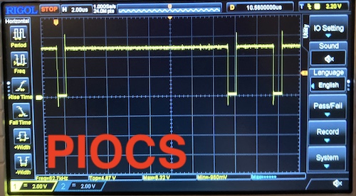
Even though the CPU is sort of running, I still didn’t get any valid composite video output. On the DE9 RGBI/CGA connector on the back of the Tandy, I noticed that H-sync and V-sync were both oscillating. The HSync seemed low at only 6.9kHz measured, but I had seen problems with the Rigol scope’s frequency counter before and didn’t trust it.
Either way, I couldn’t detect any data on the R, G, B, or Intensity pins. It seemed like the computer was generating a raster, but there was nothing to display.
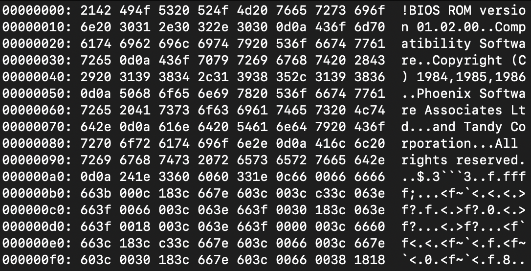
Maybe the CPU is simply not following a program? To make sure the 8079-015 BIOS mask ROM was okay, I pulled it and dumped it as a 27C128 without a chip ID check. This produced something that at least looked right in the hex editor.
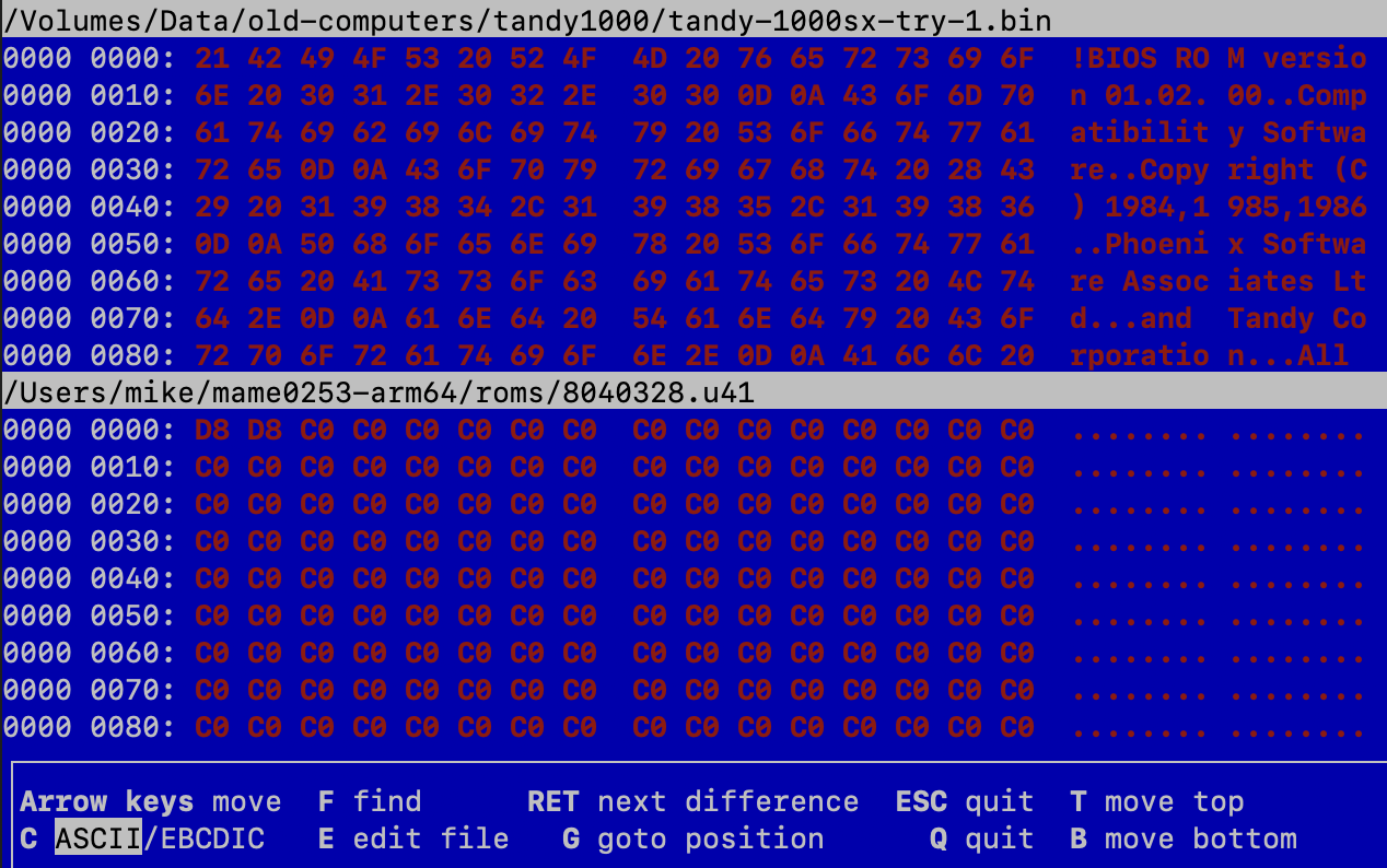
That ROM didn’t match the 8040-328 Tandy 1000SX ROM that we have in MAME for position U41. Not even close: the MAME ROM (bottom) has copyright strings at $4000 , not $0000 … and the MAME ROM is 32 kilobytes… oh.
After redumping the ROM as a 27C256, the two ROMs now looked identical, except that the MAME rom had $c0 garbage at the start and my freshly dumped one had $ff .
I tried to feed MAME the ROM that I had just dumped, and it booted right up. For sure, this ROM was valid. Now I was out of ideas.
DMA
Or so I thought. That state of frustrated confusion only lasted for a couple of hours, then I decided to take a look at another custom chip: the DMA controller. Although I know deep down that it is predictable, part of an orderly universe, and makes sense, DMA is still a little spooky and mysterious to me. If the CPU is cooling its heels waiting for the DMA controller to pick up the phone, it made sense that it could keep the system from starting.
Tandy’s DMA controller is another custom chip (Tandy part number 8075711) that integrates memory refresh circuitry, some decoding, and the better part of an Intel 8237A DMA controller. If the other big PLCC died, then why not this one?
I decided that a good first place to check would be the and signals on the work and video RAM. According to the schematic, these signals are driven exclusively by the DMA IC. If those signals weren’t oscillating, it pointed to some kind of problem in this chip, and I’d be able to work backward to blame it more conclusively.
I did see those signals, but only for “BANK 0” of the work RAM, even with the jumper pulled. “BANK 1” remained silent, which I thought was weird, as these RAMs need to refresh. I also saw the signal oscillating for both the work RAMs and the video RAM, which meant that it was being accessed. The write signal did not assert, but that’s to be expected if the computer wasn’t doing anything useful.
So, at least part of the DMA controller is working properly, if it’s able to manipulate the state of the DRAMs attached to it. That ruled out this custom chip: finally something that wasn’t blown.
Now I was really out of ideas.
Buffers
I was so desperate, that I decided I would actually look at the instructions. The Tandy 1000SX technical manual’s excellent “theory of operation” section states:
The CPU data bus is buffered by U52 (74LS245) before being supplied to the rest of the computer. The address bus is buffered as follows: 16 of 22 address bus lines are latched and buffered by U42 and U43 (74LS373). Four lines (A12-A15) are buffered by 1/2 of U54 (74LS244).
Since U52 was socketed, I figured I’d try it. Tandy wouldn’t have spent a few cents on a socket3 if they didn’t think that this part might be prone to failure. Being meant partially as a sacrificial protection against whole-board damage, buffers are a very common failure point, although I personally had not seen one fail yet. I tested these in my TL866 EPROM programmer, using the XGpro software, which has a convenient (if not always correct) logic IC testing mode. U52 passed.
There were a couple other socketed 74LS245s, so I tried them in the tester, too. U39 passed… but U40 failed. Big time. U40 didn’t seem like a particularly important part to me from the description in the manual, but the test was still saying it was bad, so it got replaced:
After being buffered, the CPU address/data bus is connected directly to the 5 expansion bus connectors. Also, the address bus is directly connected to the rest of the system board. The data bus is separately buffered by (U40) before being supplied to system board.
If I’m reading the test results properly, the chip is just straight out dead, not responding to anyone’s inquiries in either direction. That seemed unlikely to keep the computer from booting, to me. It’s also possible that some previous owner stuck in a bad ISA card way back when the computer was still working: one of the slot covers is missing, after all.
U40’s direction and chip select are controlled by a small PLD nearby, U18. U18 is also responsible for the BIOS ROM chip enable, which seemed to be working properly from the previous scoping of that line.
I decided to replace U40 with a known-good ‘245, except for some reason I didn’t have any on hand. To get one, I ended up braving the spiders in the basement to dig out a condemned Japanese Hitachi B16EX-II (utterly destroyed by a multi-cell clock battery: one of very few I’ve given up on!) and desoldered the 74ALS245 out of that computer. That chip tested out fine on the TL866, so I plugged it into the Tandy.
Still screen garbage and no boot, as expected. Time to do some more research.
Startup Sequence
To figure out what the Tandy 1000SX usually did during startup, I leaned on the MAME emulator’s built-in debugger. As previously stated, MAME has support for the Tandy 1000SX, and I had a working BIOS ROM for the system, so I made the debugger dump a line to the trace log every time the startup sequence accessed an I/O port:
> trace tandy.log
> wpiset 0000,0x400,r,1==1,{ tracelog "IO read %08X = %08X\n", wpaddr, wpdata ; g }
> wpiset 0000,0x400,w,1==1,{ tracelog "IO write %08X = %08X\n", wpaddr, wpdata ; g }
This resulted in a trace file that looked sort of like this:
FC4A8: loop    0FC4A8h
FC4A8: loop    0FC4A8h

   (loops for 478 instructions)

FC4AA: in      al,62h
IO read 00000062 = 000000FF
FC4AC: mov     dx,378h
FC4AF: test    al,10h
FC4B1: je      0FC4B7h
FC4B3: mov     al,18h
FC4B5: jmp     0FC4B9h
FC4B9: out     0A0h,al
IO write 000000A0 = 00000018
FC4BB: out     dx,al
IO write 00000378 = 00000018
I wrote a quickie Python script to parse this log and decode the I/O addresses to peripherals, according to the Tandy technical manual. Output from that script looked sort of like this, which I think we all can agree is easier to understand:
r PIO Port C 0x62 = 0xff
w NMI mask register 0xa0 = 0x18
w Printer data latch 0x378 = 0x18
r PIO Port C 0x62 = 0xff
w PIO Port C 0x62 = 0xff
w Floppy controller DOR register? 0x3f2 = 0x3
w Floppy controller drive select 0x3f1 = 0x0
r System Video address (W)/status (R) 0x3da = 0x11
r Not used 0x3ba = 0xff
w Not used 0x3c0 = 0x0
w System Video mode (clock) select register 0x3d8 = 0x20
w System Video address (W)/status (R) 0x3da = 0x3
w System Video data (W) 0x3de = 0x0
[... hundreds more]
Although MAME is never perfectly accurate to a real machine (for instance, devices are always “ready,” memory is always zeroed out on startup, things run faster or slower or synchronously instead of asynchronously) this at least gave me a rough idea of what the BIOS was looking to do during startup, and in what order.
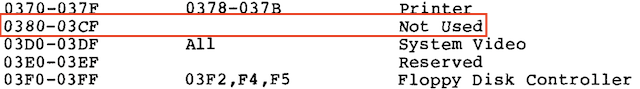
What’s up with the “not used” I/O addresses there? Well, that’s what the Tandy manual says… clearly they are lying, since the BIOS is hitting them. Not much we can do about that, though. Even the MAME driver doesn’t hook this to anything in the I/O map.
My assumption at this point of debugging the sickly Tandy was that we never “got to” the point of setting the clock for the video chipset, because we are getting basically worthless junk on composite, and a slow clock on the horizontal sync output of the RGBI connector. Flipping the dip-switch to disable internal video also had no effect on the video output, so perhaps it wasn’t even getting to the point of reading it.
Open the DOR
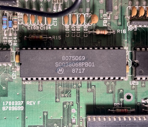
I wasn’t sure what the “DOR” register at $3f2 was, but the keyboard interface controller at U22 had an input pin marked which seemed to control access to its logic for manipulating the floppy drive controller’s configuration. Yes, the keyboard controller – another custom part (Tandy 8075-069) – handles several FDC pins in this system, including the motor line and drive select.
After a couple minutes on Google, it turns out that “DOR” is an acronym for “Digital Output Register.” Other µPD765-based floppy chipsets use this term to describe essentially the exact same control register: drive select, FDC reset, motor enables, DMA. You gotta store this data somewhere, and I guess it must have been better for yields to store it in a latch outside of the floppy controller than inside the chip itself.
Because it drives the drive select signals to the FDC, the keyboard controller is the part that ends up holding the data for this configuration register, so I would have expected it to be chip-selected when we were trying to change the contents of that register.
So, I checked to see if did anything on U22. If it was never toggled, then in theory the computer had not reached the point of manipulating the DOR register yet as part of setting drive select. If it looked squashed, then maybe the keyboard controller had also died from the overvoltage event, and it was pulling down the output from some other part and ignoring it.
never asserted when starting up the system, but the PIO select signal did, exactly three times. In the MAME log, $62 is accessed a total of 37 times, which is a slightly larger number than 3.
Neither signal looked “stepped-on,” with a strong 5V. originates from the Light Blue, where it is called “configuration register chip select.” Since I’d just replaced the Light Blue, I was pretty sure that chip was good now. I wasn’t sure if this pin would even be asserted when writing to the DOR, and it wasn’t obvious where it came from.
The block diagram for the Light Blue indicated that was decoded through some combination of the below signals:
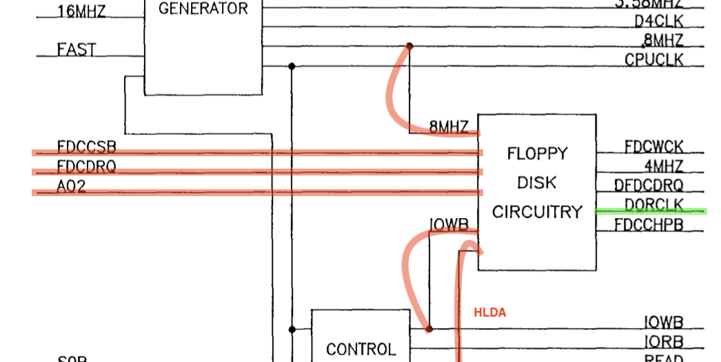
However, the information in the manual didn’t exactly explain the equation of how these signals came together, so I was unsure which signals contributed to this select. DORCLK doesn’t even appear in the (very nice) timing diagrams provided for the Light Blue.
appeared to be selected by a 74HCT138, U19, which is decoded when and AA0 are active. AA0 is provided by the Big Blue that we just replaced, and I have no idea when that signal is asserted, as it comes from a pin only marked on the schematics as “A.”
If the startup execution never made it to activate , but it made it to the PIO select that was immediately before it in the MAME startup list, then that didn’t leave too many other things on the table. Even taking into account a little bit of emulator inaccuracy, it didn’t seem likely that it would never get hit.
Based on our log, MAME hit the FDC next, to set the drive select invert feature at $3f1 . Since that’s the first hit to the FDC in the entire log, I decided to check if was ever activated during startup. It was not.
I thought about writing a custom ROM to deliberately hit the DOR register, to see if that asserted DORCLK. My skill set in x86 is pretty minimal, however, and I wasn’t enthralled at the idea of starting a whole sub-project. This would be a good application for something like a Glasgow or Fluke 9010A: connect it to the CPU socket, control the entire bus with our debugger, and poke memory to see which selects get lit up.
After reading more of the schematic, I determined that it was possible I was looking in the wrong place: the printer control custom also contained some of the FDC logic. Apparently Tandy just shoved this stuff in whatever custom they had a few free gates in.
Because the Rockwell R6765 floppy controller was getting warmer than I would have expected for a µPD765, I pulled it out of its socket, but this didn’t change anything about the boot process.
Despite the heat coming out of the floppy controller, none of the inputs and outputs looked especially bad. I was beginning to suspect there was some kind of bus fighting going on.
I dunno what happened, but…
Remember how earlier I mentioned that the D0 pin looked funny on the CPU side? I decided to pull the CPU entirely out of the socket, and turn on the computer. Then D0 on the CPU side reported 1.5V, even though nothing was being asked by the CPU to drive it. I started to get really excited at this point.
I pulled the CPU-data-bus-buffering ‘245 at U52 and replaced it with the one I just pulled out of the Hitachi, leaving the ISA-bus-buffering ‘245 at U40 now empty, and the contention on D0 dropped to 800mV.
Then I looked at the other ‘373 handling address/data multiplexing for the CPU. Its address 8 input was at 1.25V, even though no one was there to drive it anymore with the CPU having moved out of the neighbourhood.
I swapped the CPU for another V20 from the tube, and now I was getting VRAM and RAM writes. There were periodic VRAM writes, but something happened during my testing, and then they only started happening on reset. I started poking things in the board, checking random pins, hoping I could “sneak up” on the problem and surprise it. My quarry had escaped me, though.
I went to bed. I try to stop working on things after an hour without anything changing, when I’m getting paranoid, or when I otherwise notice that I am screwing up my mental model of the state of things.
After putting back the previous V20 CPU with a fresh mind and a nice coffee, I reinstalled the ‘245 at U40. I looked up and suddenly noticed that I had some video! Unfortunately, because of my poor mental state the previous night, I’m not exactly sure which series of fixes got the computer to run: I wasn’t looking at the monitor between each swap, because I was so absorbed in checking scope shots. When I looked up from the guts of the machine to take a break, the computer was producing legible video…
Even after all this struggle, I’m ashamed to say that I’m still not entirely sure what I did to make it work. Maybe something had a dirty socket? Swapping the ‘245s and CPU back didn’t make it break again.
Now, I had some actual video, and legible text! Woohoo!
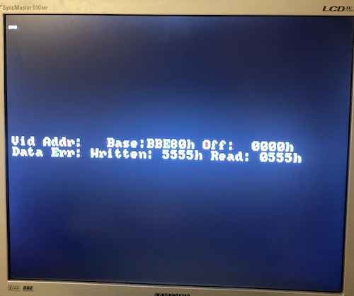
Of course, that legible text is of a cryptic error message. I’ll take what I can get at this point.
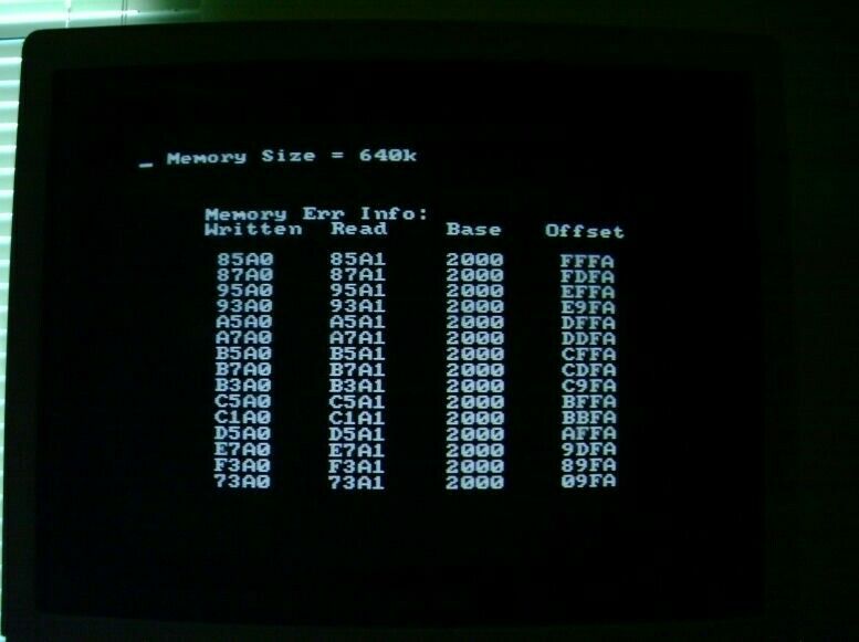
Video RAM Booboo
This message seems to indicate that the video RAM isn’t working properly. According to the MAME driver for the Tandy 1000, $b8000 to $bffff is video RAM. Another clue is that the error says “Vid Addr” at the start.
I suspected that this complaint (an entire missing high nibble!) was because I had the wrong kind of RAM in for the work RAM.
$5555 is 0101 0101 0101 0101, and $0555 is obviously 0000 0101 0101 0101. The whole top nibble is missing!
I had already replaced three out of the four 64Kx4 MT4067 video RAMs with 64Kx4 SL41464s, and three out of four sets of 4-bit nibbles were working properly… was it possible that the last surviving Micron video RAM had finally packed it in? Could I have gotten that lucky?
I tested the Micron one, it failed instantly, and I replaced it with another 41464. This time, I got a different memory error message, one that I was anticipating.
Video RAM’s fixed, work RAM’s still bad. Progress is progress.
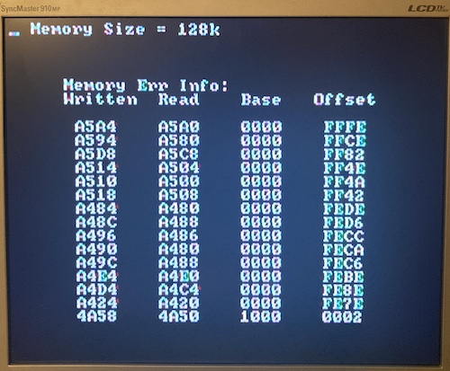
Work RAM Booboo
For whatever reason, I had convinced myself in 2019 that the 16-pin Micron MT1259 work RAM which had been fried in a previous part of the repair was equivalent to a common 4164, and so I plugged in 4164s to replace them. This was the wrong thing to do.
In actual reality, an MT1259 is a 256K x 1 DRAM, and a 4164 is a 64K x 1 DRAM. Even though both of them have the same number of pins on the package, the MT1259 uses one of the “not connected” pins on the 4164 as an additional address pin, which means it is 9 rows x 9 columns, which somehow adds up to 2(9+9) = 262,144 1-bit memory cells. Eight of them make up the 256 kilobytes of work RAM in “Bank 0.” Instead, I only have 64 kilobytes, which we can all agree is less than 256.
Up to this point, I didn’t think that this was affecting the startup. This is because I never saw the “write” pins oscillating on the chips, and if nothing ever wrote to the RAM, how could it be expected to read something valid back?
Because the universe had smiled on me at last, I now had a complete enough board, with enough parts working in harmony, for the boot process to get to the point of turning the video on and complaining about its mangled RAM. Thank you, universe.
Remember how we saw a work-RAM error message in the original ad from the seller of the machine? What a more innocent time that was. Now, even some of the good RAM in this picture has gone to Silicon Heaven, where I assure you that they don’t let toasters in.
Now that I had the RAM tester, I decided that I would re-check the MT1259s that I had previously removed as “bad” four years ago. No, I don’t throw anything out. Is this your first time reading this blog?
To no one’s surprise, the RAMs that got super hot to the touch when powered were still bad. Back in the bad chips box with you, in case someone develops a way to revive dead Micron RAM, or I need them for a Halloween costume or something.
If I wanted to get this Tandy to work, I had to find some replacements for the MT1259. According to minuszerodegrees’s 256K x 1-bit RAM interchange list, other popular kinds of 16-pin 256K x 1-bit DRAMs include many manufacturers’ versions of the 41256.
Despite being an extremely popular chip, I didn’t have any loose 41256s, not even on parts boards, and I needed at least six more of them to populate the lower bank of the Tandy 1000SX enough to boot it (assuming that the two remaining MT1259s were still good, that is.)
I was curious, though. Would it work with 16 4164s in it? Sure, the resulting 128kB of RAM would be less than the 1000SX shipped with, but it would be the same as an original Tandy 1000!
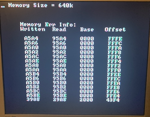
…no, that didn’t quite work. In fact, the system is so angry at me that it is rapidly changing the bottom line of the display with all the new errors it’s finding, because they presumably never thought it would generate so many errors that they would need to implement a scroll routine for this screen. Judging from the “Memory Size” statement at the top, this machine expects 256K x 1 RAMs to be installed.
An unmodified Tandy 1000SX won’t pass the memory check running entirely on 4164s. We’ve done science today, give yourself a pat on the back.
There is probably a creative way around this. Chartreuse suggested bodge-wiring a 30-pin SIMM directly onto the motherboard. You could hack the BIOS to just not bother checking. Heroically, I decided instead to sit and be grumpy while waiting for the correct RAM to arrive.
While I was waiting, I decided I would remove all the 4164s and test them before I put them back into the tube. All but one of them passed the test – I’m sure that dead bit out of sixteen wasn’t helping that memory test any, either.
Eventually, a baggie of twenty 41256s showed up from AliExpress, and I tested all of them before insertion. Each and every one of them tested out fine, so I have four left over now, which is not really a useful number of 256Kx1s.
Hold my breath, flip the switch, and…
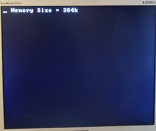
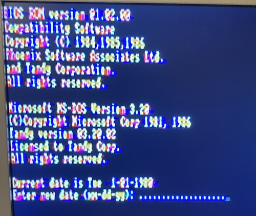
384K! I forgot to take out the E1-E2 jumper to enable the 640K. I kept watching, though, and was rewarded with, at long last, a happy boot beep. After that, the little Tandy showed the BIOS sign-on message and asked for a disk to be inserted.
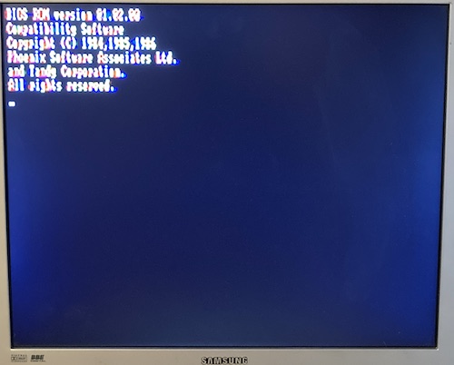
Wow, it’s actually booting the ROM now. I can hardly believe it.
So we’re in business, but now we need an operating system.
Will it boot?
I took out one of my Goteks, along with my 5.25” edge connector to 3.5” pin connector floppy adapter boards. It’s been a little while since I’ve used one of these! After some finagling and cable twisting, I got the Gotek hooked up to the Tandy 1000SX, and the Tandy started to read the image of MS-DOS 3.20 that I put on it.
Hooray! The floppy controller works, and the whole computer is alive enough to boot DOS from a Gotek. A huge step forward.
Keyboarding House
At this point, I decided to test out the keyboard controller before moving on. Blog friend Chartreuse had traded me a Tandy 2000 keyboard a few months ago (for a relatively nice PS/2 Happy Hacking keyboard that I stumbled into winning on Yahoo! Auctions Japan.)
Even given the name, the keyboard protocols are reportedly close enough that the 2000 keyboard will work on the 1000.
There was also a reference to a Tandy 2000 technical bulletin, 2000:43, which stated how to convert a Tandy 1000 keyboard into a Tandy 2000 one, which just consists of changing the 8-pin DIN into a 5-pin DIN and replacing two incorrect key caps.
Given this plethora of evidence that it should work, I decided to try it and see for myself. However, the Tandy 2000 keyboard worked very oddly: most key presses would produce a period character, but if I repeatedly pressed, say, Q, I would get a ton of . in a row and then eventually a series of Qs, before devolving back into .. This worked for a couple different keys, but not often.
Eventually, if I kept typing long enough, the computer would seem to fill up some internal buffer and just angrily beep at me while not appending any more periods. This was a little frustrating: not working at all is fine, but working sometimes?
To rule in or out the keyboard as the source of the fault, I fished out my Tandy 1000TX and plugged the Tandy 2000 keyboard into it. Remember, kids: it’s not hoarding, it’s peer review.
It acted identically there, too. Keys would work properly for awhile, and then things would degenerate into beeping and emitting periods on the DOS prompt. What was going on?
I decided to triple-check the pinouts, based on the Tandy 1000SX and Tandy 2000 service manuals. Here’s what I found:
| Pin No. | Tandy 1000SX signal | Tandy 2000 signal |
|---|---|---|
| 1 | DATA |
DATA |
| 2 | ||
| 3 | GND |
GND |
| 4 | CLK |
CLK |
| 5 | +5V | +5V |
| 6 | RESET |
N/A |
| 7 | MULTIDATA |
N/A |
| 8 | MULTICLK |
N/A |
In other words, they’re identical signals, except I’m missing RESET, which the Tandy 2000 keyboard doesn’t expect anyway.
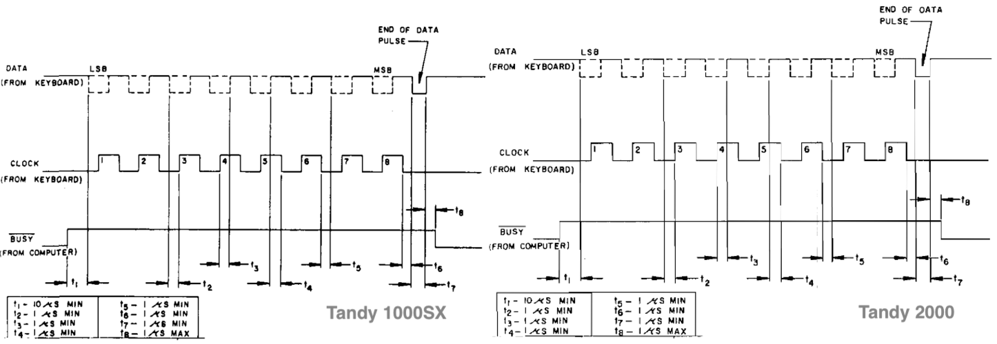
The timing diagram also looks identical. In fact, it looks photocopied.
There’s one clue that Tandy didn’t want me to do this: the right-angle plug on the Tandy 2000 keyboard is too shallow to make electrical contact with the 1000TX’s keyboard port, which lives deep inside the plastic front fascia. I had to pull the front case off the 1000TX to give it depth to seat, and I think once you are stripping parts off your computer to make it fit, you can no longer really complain that it doesn’t work.
Taken all together, this outcome was super confusing. I thought it was unlikely that both Tandys had bad keyboard controllers. To make really, really sure, I considered also adapting the keyboard into the Tandy 1000EX’s internal keyboard connector. Unfortunately, I then found out that the 1000EX directly interrogates the matrix, and integrates the keyboard controller and keyboard microcontroller both into the motherboard.
We’ll investigate the Tandy 2000 keyboard mystery at some future time. Every indication says that it should work. I decided to do something reckless to get this 1000SX, at long last, working…
Get Another Keyboard
I lucked out and found someone locally selling a Tandy 1000 keyboard. It turned out to be part of an estate sale, containing a lot of TRS-80 gadgetry. When I went to pick it up, there were a bunch of Model III TRS-80s lying around the front room, looking for new homes.
Exercising the greatest restraint and muttering the litany against starting on a whole new platform, I left only with the keyboard, which cost about the same as the Tandy 1000SX did in the first place…
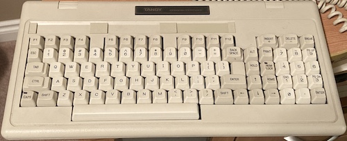
This keyboard worked on both the 1000TX and 1000SX without missing a beat!
Which is good, because everything around it failed. I broke the OLED screen on the Gotek while trying to hot glue it into the case, and my Samsung 910MP monitor decided to go on strike. As well, the HFE disk image that I made for said Gotek, containing a copy of Sopwith, wasn’t being picked up.
We’ll worry about all of that stress in a future article. After more than four years of struggle, I am happy to call this machine “fixed.” Now we just need to make it useful.
Repair Summary
| Fault | Remedy | Caveats |
|---|---|---|
| Reset is weak, no CPU clock | Replace Light Blue (U51) | |
| 28MHz clock is weak | Replace Big Blue (U30) | |
| No address bus activity from CPU | Replace 8088 CPU | CPU needs further testing to confirm if it’s actually bad |
| 74LS245 (U40) fails test | Replace with salvaged 74ALS245 | Seemed to work better if an ALS was placed closer to the CPU, and the LS from there placed in U40 instead. Swapping them back did not make the failure re-occur. Not sure what’s going on, may fail again. All three have since been replaced with brand new parts |
| “Vid Addr” VRAM error | Replace blown MT4067 video RAM with 41464 | |
| “Memory Err” memory error | Replace 4164 main RAM with 41256, including damaged 4164 | |
| Tandy 2000 keyboard not working reliably | Replace with Tandy 1000 keyboard | Tandy 2000 keyboards should work, is the keyboard broken? |
-
In real mode, like what the 8088 starts up in, you can easily convert between segmented (
segment:offset) and physical addresses by using the formulaaddress = segment * 16 + offset. In protected mode, things are a little more complicated, but luckily we are on an 8088. ↩ -
Why buffer address lines at all? Other than the obvious protection that it lends to the CPU if something goes wrong, the primary reason is to provide reliable current sourcing for the rest of the board. If you think about all the places that a popular address line like A14 might go on the board, you can imagine that there’s quite a lot of current being pulled from the CPU through some very thin, long traces, past sources of noise. This concept is known professionally as “fan-out.” Better to let something big, cheap, and dumb like a 74LS244 provide that current on its behalf, and let the NMOS 8088 worry about keeping heat down and speeds up. ↩
-
The Tandy manual actually says that only U52 is meant to be socketed: U39 and U40 also have sockets on my board, but they look identical to the somewhat unusual-looking OEM sockets, so I don’t think this board has been reworked by a previous owner. Otherwise, I would be much more suspicious that a socket or trace had failed during the rework. ↩