Dogfighting the Sharp X68000 ACE
Tags: sharp x68000 x68000-ace corrosion capacitors repair homemade-hardware trace-repair failure
When we were first introduced to the X68000 ACE, we saw that the board was very corroded from battery damage. Later on, I whacked the battery out of it and did my best to clean up the corrosion without completely dismantling the machine. This time, it’s personal. Workstation, that is.
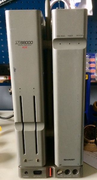
My initial assumption was that all I’d really need to do is get the I/O board out and repair the obvious battery damage. But, as we all know, old plastics can conspire to slow you down on a project. In the end, the system still isn’t working properly, but it’s come a long way.
I had sat on this project for a few months/years, because it doesn’t really have a satisfying conclusion, but I decided that it would be better to publicize my struggles. Maybe it’ll help you fix your own X68000!
Taking It Apart
As you might recall, a twin-tower X68000 consists of two major boards:
- The mainboard, which contains the RAM, BIOS ROM, various custom chips, and the CPU;
- And the bottom board, which handles a lot of the 8-bit I/O (SASI, FDC, serial, etc) as well as containing the clock battery.
There’s an number of other sub-boards in my system, such as the one that breaks out the external SASI port, the analogue video output board, and the RAM expansion, but those aren’t really important today.
My goal here was to extract the bottom board from the system so it could be cleaned up.
Getting the bottom K5710DE “I/O” board out of the twin-tower X68000 ACE is nowhere near as hard as I thought it was. After looking at a YouTube video, I realized all I had to do was disconnect all the cables from that bottom board, and then remove two screws hidden at the rear of the ‘spine.’ After that, the five screws on the bottom of the machine came right out, which releases the bottom plate and board from the plastic bits. The board is screwed to the bottom plate of the case with three easy-to-remove screws.
Then all you have to do is awkwardly lay the rest of the system on its side, and try not to scratch the plastic any worse.
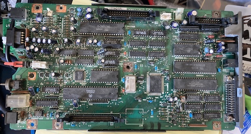
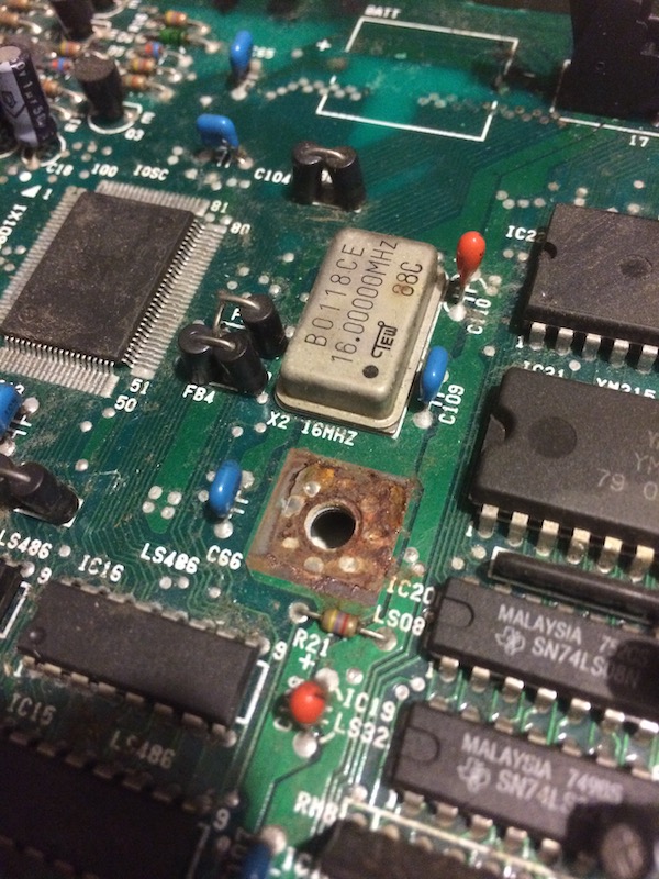
All of the exposed copper meant for grounding to the screw holes is corroded, with some of it having gotten a big dose of battery acid and corroding even further. The one in the centre is especially bad:
On the initial inspection, I missed that the pin header that goes to the hard drive (SASI) breakout board got corroded as well. Although the connector cleaned up with some alcohol, there’s some green crap all the way up inside the ribbon cable, which probably necessitates a brand new replacement in the future:
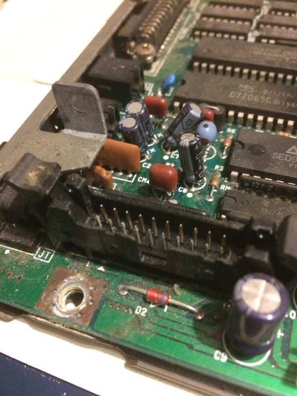
I marked the cable with an “X,” so I wouldn’t be surprised later when it came time to put a hard drive in it.
The bottom of the I/O board is surprisingly clean, with only a few spots covered in some kind of dusty white corrosion that seems to be not uncommon for machines stored in Japanese humidity.
Just like on the X1turbo, Sharp’s engineers put the I/O-board silkscreens on both sides to aid in diagnostics. Thank you!
Most of the actual gunk seemed to just be old flux on the ports, but I noticed a suspicious amount of dirt far away from them, especially on the bottom of this trim cap:
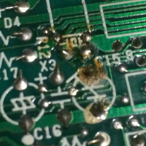
This was probably a hand-soldered part. It cleaned up fairly well, and left no indication of damaged traces behind.
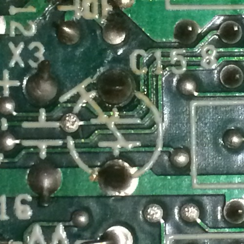
On the topside of the board, nothing looked suspicious, although this whole assembly is very close to the RP5C15 time-of-day chip that gets fingered for a large number of soft-power-related failures:
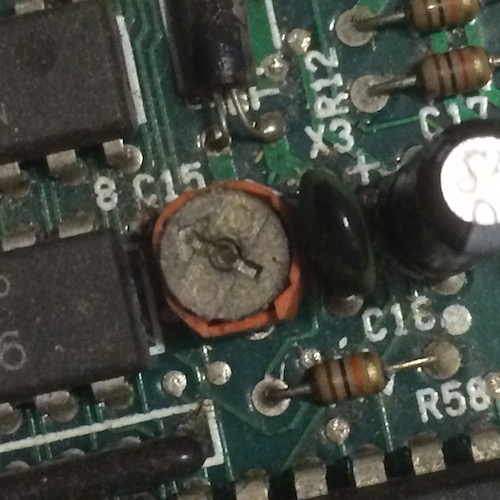
Trace You There
One thing that I noticed is that there was a lot of solder-resist damage on a thick trace running near the battery. When battery corrosion gets really bad, it damages the connection between the copper and the green solder mask, lifting it.
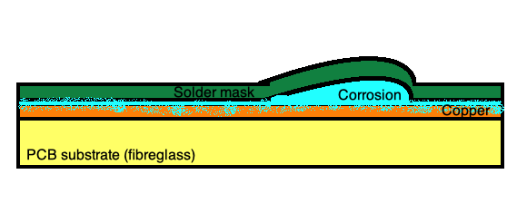
In other words, it rusts like a car does - from the inside, so as soon as you notice a paint bubble, it’s often too late for the metal.
I started probing around here to try and figure out where this thick trace that passed under the original GB50H-3 battery goes. Eventually, I started scraping off the damaged solder mask with an old Olfa blade, until some bare copper was revealed. I checked with a multimeter to see if it was working at all. Everything was electrically connected here to its destination, so I did some more scrubbing, tinned it, and made a note to cover this in UV solder mask later. This isn’t where the fault is, but it sure looks dramatic.
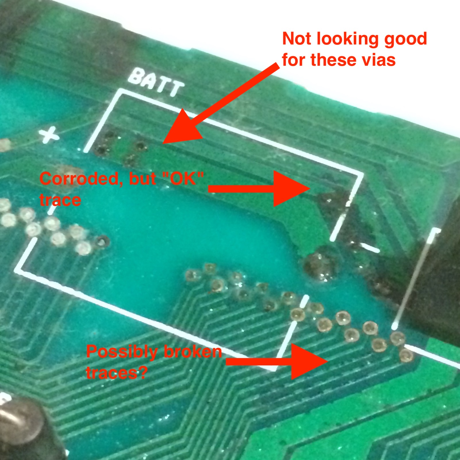
There are, however, a lot of vias in this general area that run between the major backbone ribbon connector (I call it the “Big Ribbon,” for lack of an official service manual term) and IC13, a 100-pin Sharp proprietary QFP in the middle of the I/O-board called the “IOSC.” From what I can tell of looking at a similar chip on the official XVI schematics (the ACE ones are unavailable,) this part seems to jam together a lot of interface duties for things like the floppy drives and SASI hard drive. Important, in other words.
I wanted to make sure these traces were all OK before buttoning the machine up again and beginning on the power supply repair, which at this time I had not begun. A handful of those vias buzzed out to the IOSC directly, but a lot of them were so corroded with chalky, gritty grey solder globs inside them that they were no longer conductive. The vias themselves still seemed to be intact, as I could buzz a handful of the pins on the 68-pin “Big Ribbon” connector all the way to pins on the IOSC chip, but not all.
I figured it was possible that I had corroded traces broken away from the vias, but but without being able to check all the vias, I couldn’t test them to be sure. On top of that, the compromised solder plugging those vias could be holding battery electrolyte that would eventually eat the copper in them - and then I’d definitely have to be able to clear them out to run a patch wire bottom-to-top. And that would just be a ton of work nobody wants to do, right? Right???
Dismantling and Cleaning
After looking at the I/O board, I put the machine back together and put it on the shelf for a few months. Without a schematic or a place to put all the guts of the machine while I had it dismantled, fixing the I/O board seemed intimidating.
I moved on to the power supply, and that meant there was a lot of cleaning involved.
One obvious issue is that the power supply is clogged solid with dust. It left big black streaks of grime behind on the plastic, probably because the fan is too choked to function:
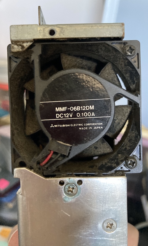
Hopefully the dust absorbed some of the capacitor goo that is surely inside this thing.
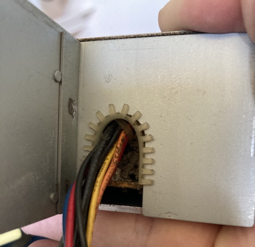
I noticed some other interesting things during the disassembly, like the floppy ribbon being attached with velcro:
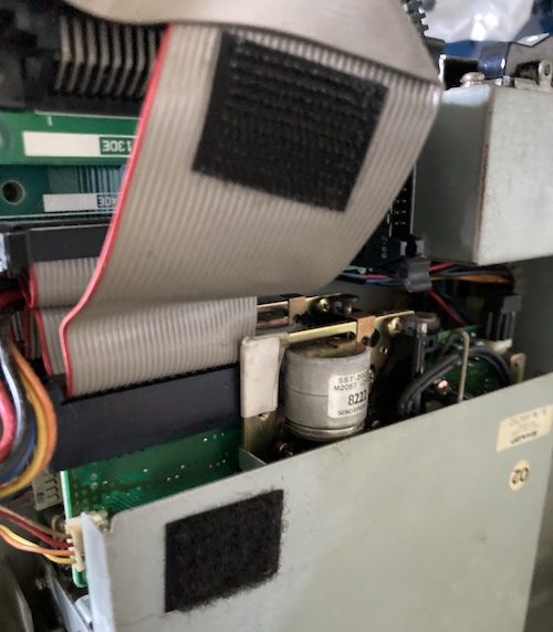
After removing the PSU and floppy drive and external hard drive breakout board, I noticed that the internal speaker is bolted to the inside of the plastics of one of the “twin towers:”
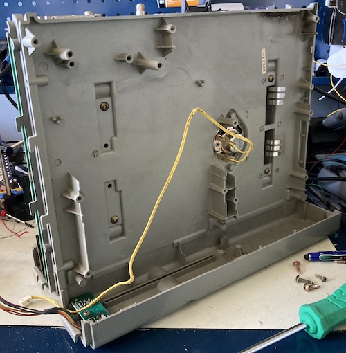
The “pop up” handle in the middle has this cool-looking pogo stick part that also holds the two halves of the case together:
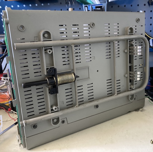
The piston in mine must be gummed up, as I’ve seen videos where it has a smooth easy action with some “easing.” Mine judders from position to position and won’t smoothly retract without lots of force. As you can see, I’m also missing one of the little plastic “feet” that keeps the handle action feeling good on a desktop. Maybe a good excuse to buy a lathe?
Motherboard comes out
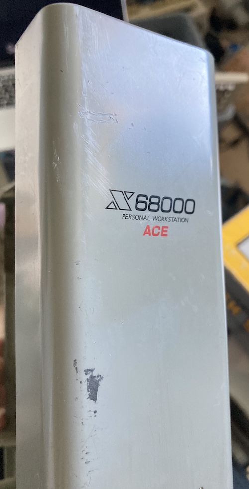
You have to remove the front fascia to get at the motherboard, as it has a pretty complicated three-piece RF shield. Here’s an absurd-resolution picture of just how bad my case plastics are:
You also have to remove the expansion card cage. Luckily, it is easy to unscrew because they left these nice reliefs for your screwdriver.
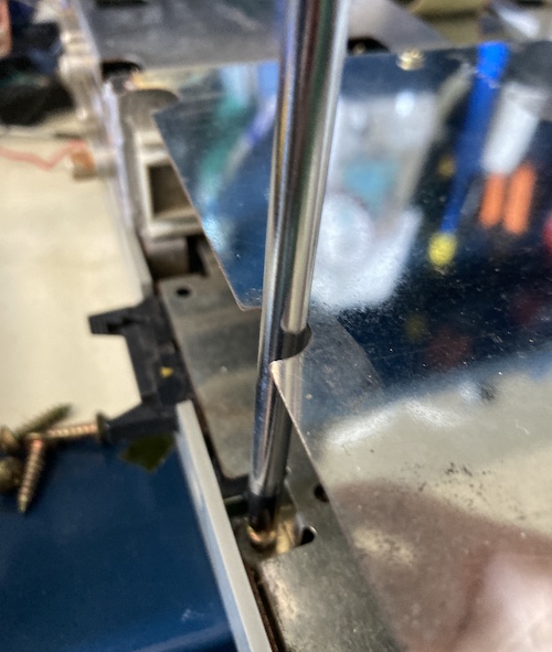
However, the whole cage is on a massive 100-pin 2-row pin header which is very nerve-wracking to undo:
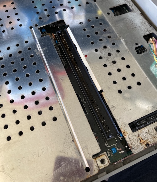
The RF shield was bouncing around the whole time; it’s very thin metal, and seems to have warped with heat and age.
The motherboard has a lot of interesting stuff too, like the Messiah. So that’s where he was hiding all this time. Someone tell the Pope.
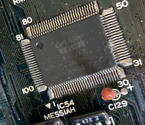
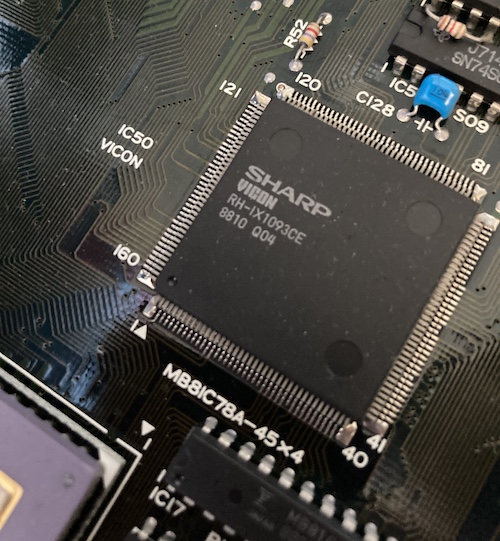
Our Messiah hangs out with a video controller chip called, unimaginatively, Vicon:
The 68K and HD63450 DMA controller are hanging out in the extreme corner of the motherboard, which seems like a weird place to put it since generally you want a CPU to be, well, central. For some reason, the 68k is thankfully socketed.
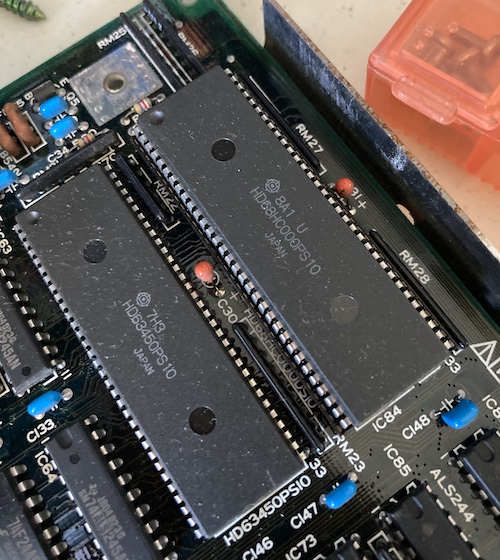
I noticed that these custom chips near the “IMDRAM” have some solder-bridged pins, but based on their position they are probably power pins, and the bridge is deliberately caused by the solder mask.
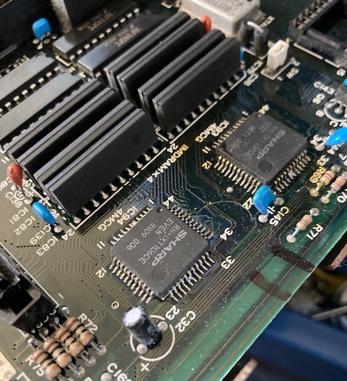
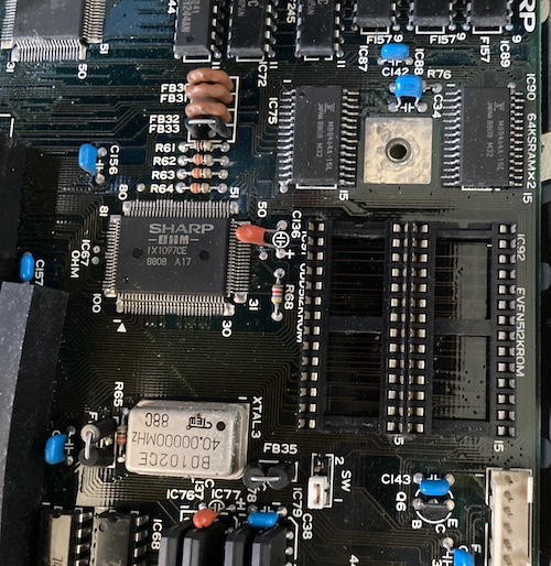
I also saw these empty ROM sockets, which say they’re for “512K ROM” odd and even. Like in the X68000 PRO, this lets you run an alternative BIOS1. The original chips are soldered in, and the nearby SW1 jumper no doubt changes which set of chips the select signal goes to.
That sinking feeling
With all the plastics removed, I scrubbed them down in the sink. Tons of grit and grease came pouring off of every single one of them, and so I gave them a quick vacation in the sun to dry before 303ing the plastic. It’s still in not-great condition (lots of chips to the paint and damage on the edges) but at least now it’s not as gross to touch.
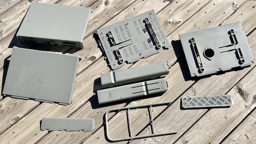
I counted over 100 screws on disassembly, which rapidly overwhelmed my ability to keep them organized. A very complicated case!
While I was waiting for everything to dry, I replaced the missing and torn feet on the metal bottom of the case with 3M SJ-5012 half-inch rubber pads in black. They are pretty much identical to the original feet, right down to the taper, which makes me wonder if it might actually be the original part.
Since the light grey plastic had so many dings and scratches in it, I also gave it a quick treatment with Novus plastic polish. The jury is still out on whether it looks a lot better, but it definitely has reduced some of the more obvious scratches and made the sides mostly shiny again.
To fully restore the aesthetics would require some fresh paint, as the paint is very badly damaged in parts and down to bare plastic in several places. Then I’d need new stickers and labels! If I can put this thing back together and have it running at the end of all this, it’s good enough for me.
Power, Supplied
At this point, I put everything else aside to focus on building a “new” power supply for the X68000. Feel free to take a departure and read about how that went.
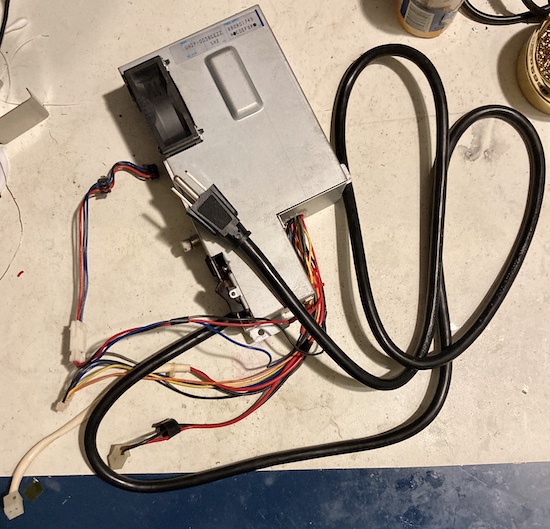
In brief, a PicoPSU adapter board was assembled with an onboard AC/DC converter inside the existing power supply case, so that the computer retained its original feel and layout. It worked well!
Hold My Battery
Another side quest was embarked upon at this point.
As I mentioned before, the original battery for the X68000 is a rechargeable NiCad.
Coin cell batteries are much less likely to leak than a NiCad barrel battery, although it’s still very possible and has happened to me in the past. With a holder, at least I can remove the battery if the computer goes into storage for a very long time in the future.
Electrically, I was nervous about choosing a 3.0V ML2032 or 3.6V LIR2032 battery for this because the charge methods differ between the original NiCad cell and the lithium-ion chemistry. The last thing I want is to trade NiCad damage on my I/O board for much more reactive lithium corrosion.
After doing some research, the datasheet for the SRAM chip (MB8464A-15L) says that I only need 2.0V to keep it alive, so a non-rechargeable CR2032 with a diode to block the recharge functionality should work very well.
I spun up a quick PCB (very cheap on Osh since it’s tiny) and then put it together. It uses an 0805 Schottky diode to try and minimize the voltage drop, but even a “regular” amount of diode drop is okay because, as I determined before, the SRAM chip only needs 2.0V. This was my first time installing a surface-mount diode, so I had to squint to figure out on which side the cathode line was.
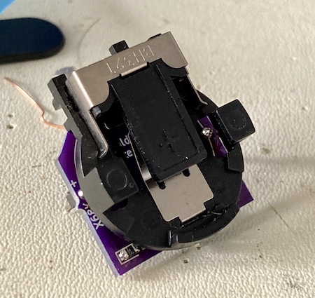
It would have been nice to make this PCB a little bigger, because it turns out to be pretty wobbly all around. The original battery holder has three points of plastic that contact with the motherboard for bracing, but the PCB only has the two electrical contacts.
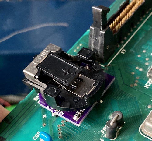
It will be annoying in the future to put a battery in or take it out of the holder because of all the wobble, but that’s better than leaking. If I get back in here, I’ll probably put a bit of sticky tack in to provide a little bit of support to the PCB.
Pleased that it fit, I didn’t solder it in, because I knew I’d be messing with the board underneath. And here’s why…
Scraping The Bottom
The I/O board still needed to be repaired. I figured I would start by scratching off the contaminated solder mask, and getting the corrosion and battery electrolyte out of the copper traces.
Even though this trace looks very bad, it is still continuous with extremely low resistance. The fibreglass pencil removed a lot of the contaminated solder mask, but it wasn’t good at removing the rest of the solder mask, unlike with the Amiga 2500, where most of the solder mask came right off within a few swipes. I ended up scraping a lot of it off with a dollar-store box-cutter, which was a harrowing experience until I got the feel for it.
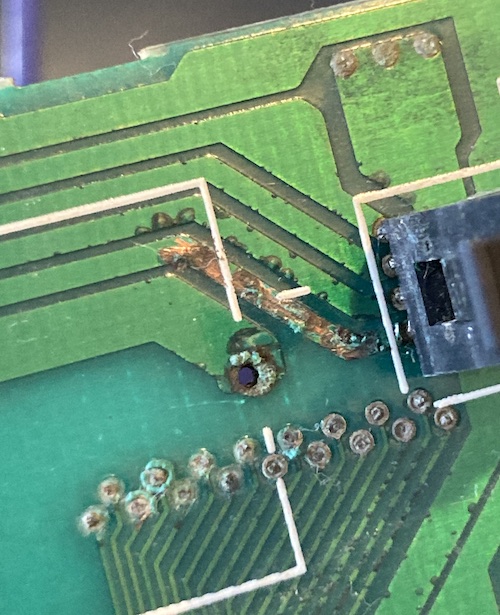
After about half an hour of very slow work, I got to see these hard brown spots in the copper. I wasn’t sure if this was contaminated copper that would start oxidizing again, or if it was just fibreglass substrate where the copper had totally worn away. It wasn’t conductive, so I suspected the latter, but I wanted to make sure.
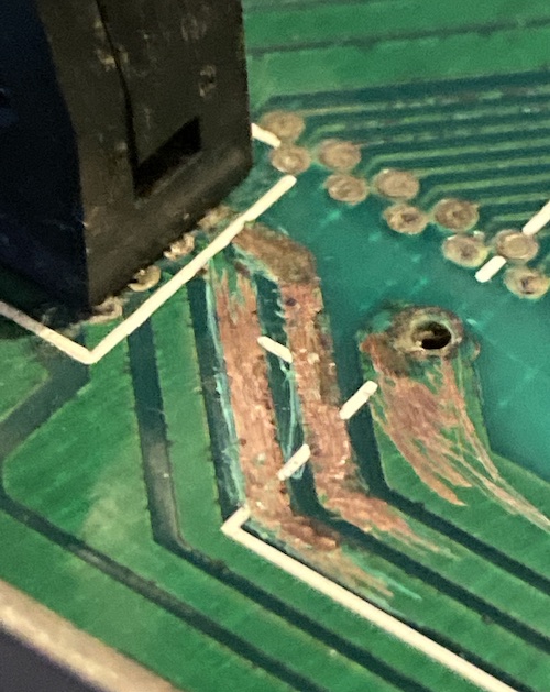
The negative battery-terminal trace on top has been severed entirely by the damage - the eyelet on the top is completely corroded. There are rivets that you can install to fix a torn plated through-hole, but I didn’t have any or the tools to install them (now corrected,) so a quick patch wire from the negative battery terminal to the vias will return the battery to proper function for now.
We’ll worry about that when it comes time to install the aforementioned coin-cell holder. I want to keep a battery in here so that the boot SRAM (where you load drivers, not just clock and configuration - more on this later) will continue to work.
Once I was somewhat satisfied that the big traces wouldn’t turn back into green nightmares, I turned my attention to the IOSC vias.
Plugging away
I worked for a couple of days on and off to try and clean out the chalky, corroded vias on the I/O board so I could test out the traces from the 68-pin “T” connector to the IOSC chip, including buying a pointier tip for my soldering iron to better direct the heat so I could “burn out” the gunk inside.
This was a lot of fiddly work, and very discouraging as at the end of most days I had no concrete improvement to show for my effort. Eventually, though, the vias were cleaned enough that I could get continuity from the vias to the “T” connector, verifying that the traces on the underside of the board (and the vias themselves) were intact. All 17 vias now buzzed out just fine top-to-bottom, which made me feel a lot better.
Unfortunately, things weren’t as good on the other end of the circuit. Only 8 out of the 17 vias were continuous with the IOSC chip. I would have preferred it the other way - it’s much easier to solder to the through-hole “T” connector than it is to the very fine pitch IOSC chip! Before running some patch wires, I wanted to verify that the traces were in fact bad. If there was just a small portion of the traces that I could clean up and fix, then that would be much easier than trying to bodge-wire onto the legs of the QFP.
I suspected the damage on the traces must be very close to the vias, since that was where most of the battery electrolyte and blue-green corrosion was hanging out. Even a very thick copper trace must become thinner when it approaches a via, and it’s well-known in the PCB manufacturing community that T-shaped intersections and 90-degree turns are notorious for trapping acid.
It took me about an hour to trace out where each via went. I took a high resolution picture and used a paint program to draw lines, which took awhile but is a lot less less error-prone than doing it by hand:
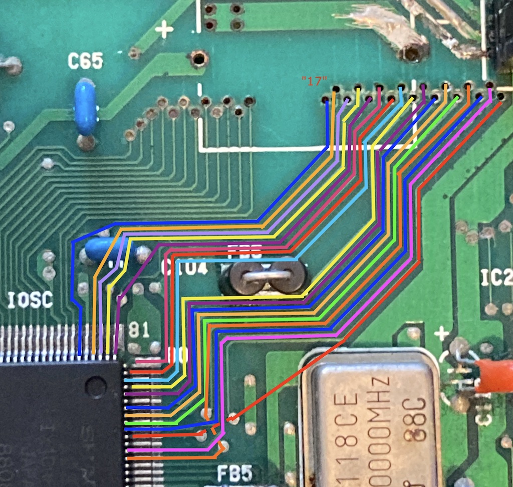
All of the pins that had additional vias nearby the IOSC were continuous from that via to the IOSC. Did that sentence make sense? Either way, it meant that the damage was closer to the vias, as I had assumed. Some of the pins, like the one I labelled “13,” were obviously obliterated.
After scraping back a little bit of the solder mask using an Olfa AK-4 knife (I can’t believe I used a box-cutter for so long for this - the Olfa is delightful) my theory was confirmed. Part of the trace is simply missing.
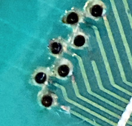
The exposed copper part of that trace buzzes to the IOSC no problem, but it isn’t connected to the via. I was correct in my initial guess that it has severed itself at the via end. So at least the required patches are short… but they’ll be pretty close together, which is a hell all its own.
The Way Back Out
On previous repairs, I’ve patched point-to-point using Kynar wire or cut-off component leads. On this I/O board, however, these traces are thin and close together, so I decided to try another route.
On the suggestion of some friends, I decided to buy some very thin magnet wire from AliExpress to patch these traces - since it was cheap, I ordered both 0.2mm and 0.3mm as my existing 0.5mm seemed too thick, although I ended up waiting so long for shipping on it that I ended up ordering another reel of 38 AWG (0.127mm) from Amazon, which of course immediately caused the AliExpress order to show up the next day.
The moral of the story is that if you’re reading this paragraph and think you might want to repair traces in the future, go order some magnet wire from AliExpress right now and it might show up by the time you get your next broken PCB.
Since it was my first time using magnet wire to patch traces, I picked up a syringe of paste flux (MG #8341). The idea I had was that the paste would add some height, so that the wire would be completely immersed when it was being soldered on and it wouldn’t matter as much about being able to hold the wire firmly and flatly to the board while soldering it. This way, the flux would provides surface tension that would help the melting solder to pull the wire flat onto the board.
This lengthy video by Branchus Creations has a fantastic zoomed-in view of the wire adhering, which gave me the confidence that I was on the right path.
When I actually went to do the patches, I first tried with liquid flux. It was really difficult to get a good adhesion. It only occured to me here that in addition to the height, the paste flux obviously contains way more flux per drop, because it doesn’t spread out and try to run away from the part that I’m working on. I’m a convert - I only wish it were easier to store the syringe.
To do the patch wiring, I cut off a ~2cm length of magnet wire and then stabbed it through each of the vias. Then, I filled the vias with solder, so that it would be conductive with the wire and also hold it in place. With the wire held tightly, I could bend it on the top side to meet the exposed copper of the trace and solder it down.
This makes it sound much easier than it actually was, because the wire is annoying to remove the coating from in practice (tin both the trace and the wire first, if you can) and everything is super small and hard to see without magnification. Before I figured out what to look for, I had a lot of trouble predicting how long I would have to keep the iron on to get rid of the coating so it would become “continuous.”
It gets worse if any contamination is kicked up from the rest of the board, because that obscures the traces even further and forces you to take a break to clean. It took me about forty minutes to do the first trace, and then the subsequent ones were a little faster. Occasionally I would bridge one trace to the one I had just done by using a bit too much solder, which necessitated some re-work. At one point I actually dropped the entire wire back out of the via for the “#1” trace, and had to redo the entire job.
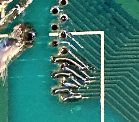
Here is a photo after I had repaired six traces. It looks ugly zoomed in, but it’s difficult to notice this detail with human eyes. I reflowed the joints after this and tried to make it look okay with a magnifying visor, but I found it really hard to produce a good clean smooth joint.
I’ve gotten a little bit better at trace repair in the years since I did this job, but not a whole lot better.
One thing that really helped was to glob up the soldering iron tip with solder and then run it along the wire and pad while holding it in place with tweezers, like when I’m drag-soldering SMD chips. Unfortunately, I only figured this out near the end.
I started on the vias at the bottom of the photo, and you can tell that I made the wires and their contacts too short. Part of the secret to making this look good and have a long-term reliable connection is to have a large “surface area” where the trace joins to the wire.
I was sure to scrape off and patch past the black corrosion that you can see on the furthest-top trace. Although they were still continuous, you could see some gunk getting exposed as the mask was scraped off:
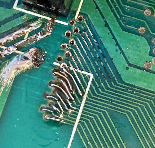
I think a cool way to repair this (which might potentially be profitable as this damage is common on early X68000s) would be to make a flex-PCB that would pin into the vias and then let you tin some exposed traces onto the original traces. Sort of like an iron-on transfer.
In any event, all of this is going under solder mask for protection, so as long as it’s got a good connection, I’m reasonably pleased.
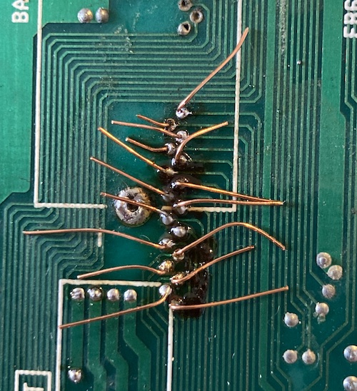
The backside produced a lot of sticky black goo which I think was a mixture of flux, leftover battery electrolyte, corrosion from the inside of the via, and the enamel coating of the magnet wire. Gross! But it wiped off with some effort. I clipped all these wires later, of course, but they were useful for testing and to keep from pulling the wire out of the via while I was soldering the other end.
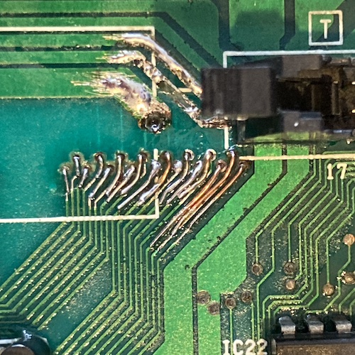
At last, all of the obvious I/O board patching was done. Each wire buzzed out between the T-connector and a pin on the IOSC, the pins seemed to go in vaguely ascending order, and there were no shorts between pins. I don’t want to add up how long this took.
For the first test, I didn’t seal this up with solder mask or install the battery holder. If it turns out I had missed a spot, it would really stink to have to remove all of that stuff in order to get back to these traces.
Now to fire up the computer! Let’s go!
Reassembly
Reassembling this thing was intimidating. As I mentioned earlier, it had been a few months since I took the computer apart, and it has dozens of screws.
I did what I always do when confronting something that makes me nervous, and I made a list.
Top of that list was to get the piston action to be less “juddery.” Although I didn’t plan on often using the carrying handle, what’s the point in tearing the machine all the way down to this point without touching it up while it’s easy? I dripped a bit of 3-in-1 oil into it after picking out a couple chunks of dust and hair from the track that the spring cup glides in. The same slow action continued but now it was much smoother.
One big mistake that I made, because of my terrible screw organization when ripping the computer apart, was taking the three fine-thread M2 screws meant for mounting the motherboard to the threaded inserts in the case, and mixing them up with the two coarse-thread M2 screws meant for mounting the speaker to the case plastic. I ended up stripping out both of the speaker holes in the case plastic - they must be the right screws, they’re in the bag with the speaker! Yeah, I put the speaker on a corner of my desk before bagging it up and that’s where I also placed the motherboard mounting screws.
To repair the now hogged-out screw holes, I ended up filling the holes with super glue. After some more experimentation, I determined that these were “thread-forming screws” and would need a pilot hole drilled in order to work effectively. The smallest drill bit I had on hand was 1/16”, which at ~1.58mm was pretty close to 2mm.
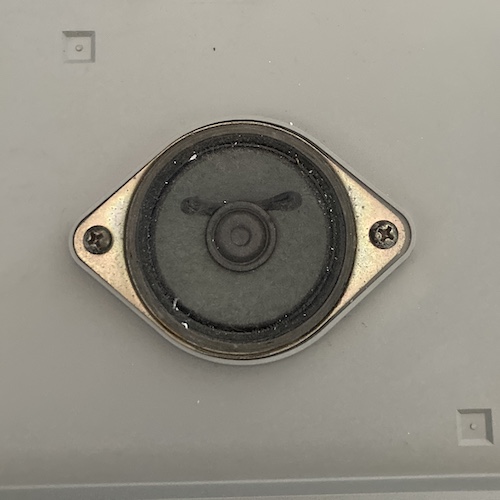
Once the pilot hole was drilled into the set super glue, I was able to thread in a screw. I wouldn’t trust this to hold any serious torque or weight, but it seemed to be enough for the speaker. We’ll see how this holds up - a better repair method would be to use some kind of plastic-compatible epoxy because super glue is quite brittle.
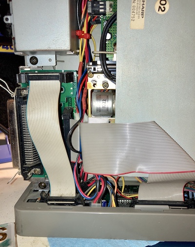
When reinstalling the floppy drive, I found out that my newly-spliced floppy power cable was now actually too long compared to before. This was sort of a nice problem to have; I ended up airplane-looping it behind the SASI breakout board to take up some slack. There’s quite the mess of wires in this computer in general:
I noticed that due to the rust on the metal parts of the case, or possibly a previous owner, or more likely incautious removal on my part, some of the brass inserts were cross-threaded and difficult to get the fine-threaded screws in properly.
I kept having to take screws out and put them back in, because later layers reused the same screw holes. There are some screws (namely the SASI breakout screw at the back) that hold in four or more major components. No wonder I had such an annoying time taking this thing apart! Finally I triumphed (of a sort - I was short several coarse-thread plastic screws and long several small fine-thread machine screws) and was able to stand the machine back up as one discrete unit on my desk once again.
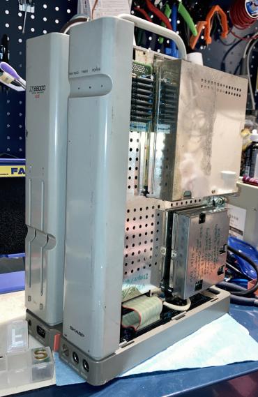
At which point it creaked like an old house for about 20 minutes, as all the plastics had expanded during their month of freedom on my workshop floor, and now were a little grumpy at being back with their partners of 30-plus years. Sure looks nice with the freshly polished case front, though!
Testing
I’m not going to lie: I was intimidated. Few things would be worse than spending all this time, effort, and money, and then watching this machine smoke one of its bespoke components. It wasn’t like it was thoroughly tested in Japan, either: it could very well have been dead before it got to me and my repair of the IOSC traces wasn’t the only problem.
In the initial test, since I didn’t have any high-density 5.25” diskettes, I would be looking for the following things:
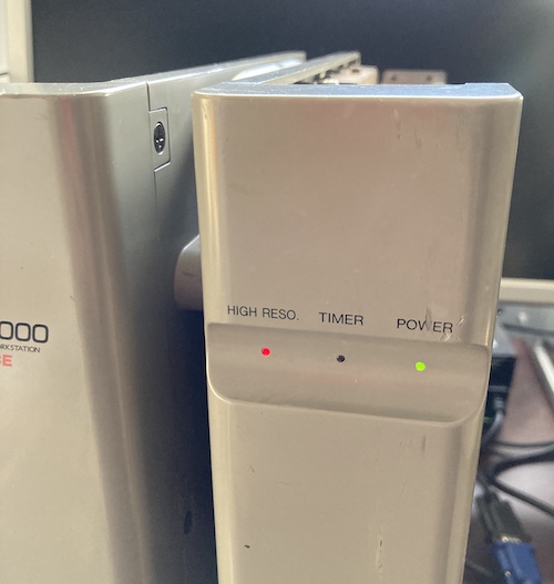
- Red light turns on when the machine is plugged in and switched on, but not powered on;
- Green light turns on when the soft power toggle button on the front is pushed;
- Video is generated;
- …and a legible “insert disk” message/logo is shown!
I did have a boxed retail copy of Klax that I got from the Suruga-ya in Shibuya, but I didn’t really know if it actually worked, nor did I know if my untested floppy drive would just rip the magnetic coating off the disc with a misaligned head. Best not to test with irreplaceable disks.
After cleaning the desk off so there was a place for it to sit, it was Halloween of all days. Perfect for some spooky behaviour!
I connected it to power and turned the hard power switch on, and saw that the red power light was on.
I pushed the power button on the front of the computer. The LED changed to green, and the computer leapt to life!
…And showed a screen of garbage amongst a message in Japanese:
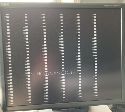
Garbage in… 31kHz? That can’t be right.
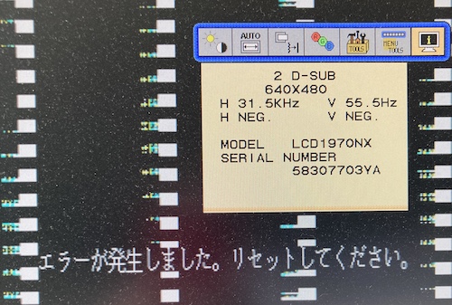
The message basically translates to “an error has occurred, please reset.” I half-expected to see this from corrupt (battery removed) SRAM. Pushing the reset button on the top of the case, I got the message again, except now without the corrupted tiles. Hmm.
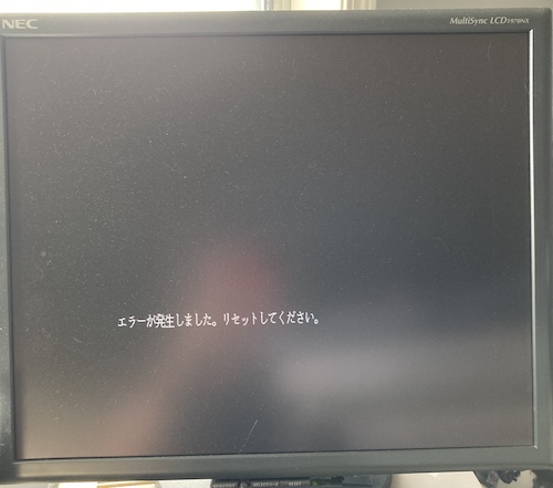
I didn’t think the video being off-centre was that relevant; this monitor can interpret seemingly everything but sometimes it shoves the video into an inappropriate corner like it’s an Amiga or something. A little horizontal and vertical position adjustment always makes things look better.
I pushed the button on the front to turn the computer off so I could plug in a keyboard, and it didn’t turn off. The power LED turned completely off, rather than blinking, and the screen stayed bright and happy instead of slowly fading out to blackness like a normal soft-power-off situation should. Uh-oh.
After a bit more nervous poking of the reset button, I saw that sometimes the reset made the screen fade out. I wasn’t sure if this was intentional behaviour, but it didn’t always come back from that. Something’s really wrong.
I shut the machine off hard, installed the keyboard, and held OPT1 on startup to reset the SRAM. Nothing changed - the LED in the “Roman characters” key would flicker for a split second on reset but this wasn’t the problem. I tinkered with the machine a bit, removing and installing parts that were easy to get to (e.g. the RAM card and floppy cables) but nothing changed. Even letting it sit for 15 minutes under power to try and reform any marginal electrolytic caps didn’t help.
At this point, I decided to check if the floppy drives would work at least, and stuck a brand-new double-density disk into the primary (#0) drive as sacrifice. The drive happily slurped it up (nice) and the LEDs on the front turned on to signal a disk had been inserted (awesome) but the drives refused to eject it (oh no.) All I’d get when I pushed the eject button was a blinking LED, some motor quivering inside, and no disk ejecting. Uh-oh. My guess is that since the eject process was doing something, it probably wasn’t software or the IO controller blocking it, but some kind of mechanical problem inside the drive - old grease or whatever. It can wait.
So, at least four new problems:
- Soft shut down doesn’t work;
- Whatever that error message is;
- Whatever that video garbage is
- Floppy drive #0 won’t eject;
Looking on the bright side, at least there’s a visible raster and it’s loading Japanese characters from the ROM! A lot of stuff has to go right to get this far.
It was probably time for some actual troubleshooting. Because I had just been monkeying in that area, I immediately thought I must have missed a broken trace or some other damage on the I/O board, probably also involving battery damage on the circuits between the “T” connector and the IOSC chip. At least it’s really easy to remove the I/O board, as opposed to almost any other component of this machine.
Fruitless fixing
I’ll save you the several weeks of frustration that followed. I tried a little bit of everything, with no real change in behaviour. One thing to watch out for are the aforementioned saggy RF shields: at one point I created a +5V to GND short using the motherboard’s RF shield as a jumper.
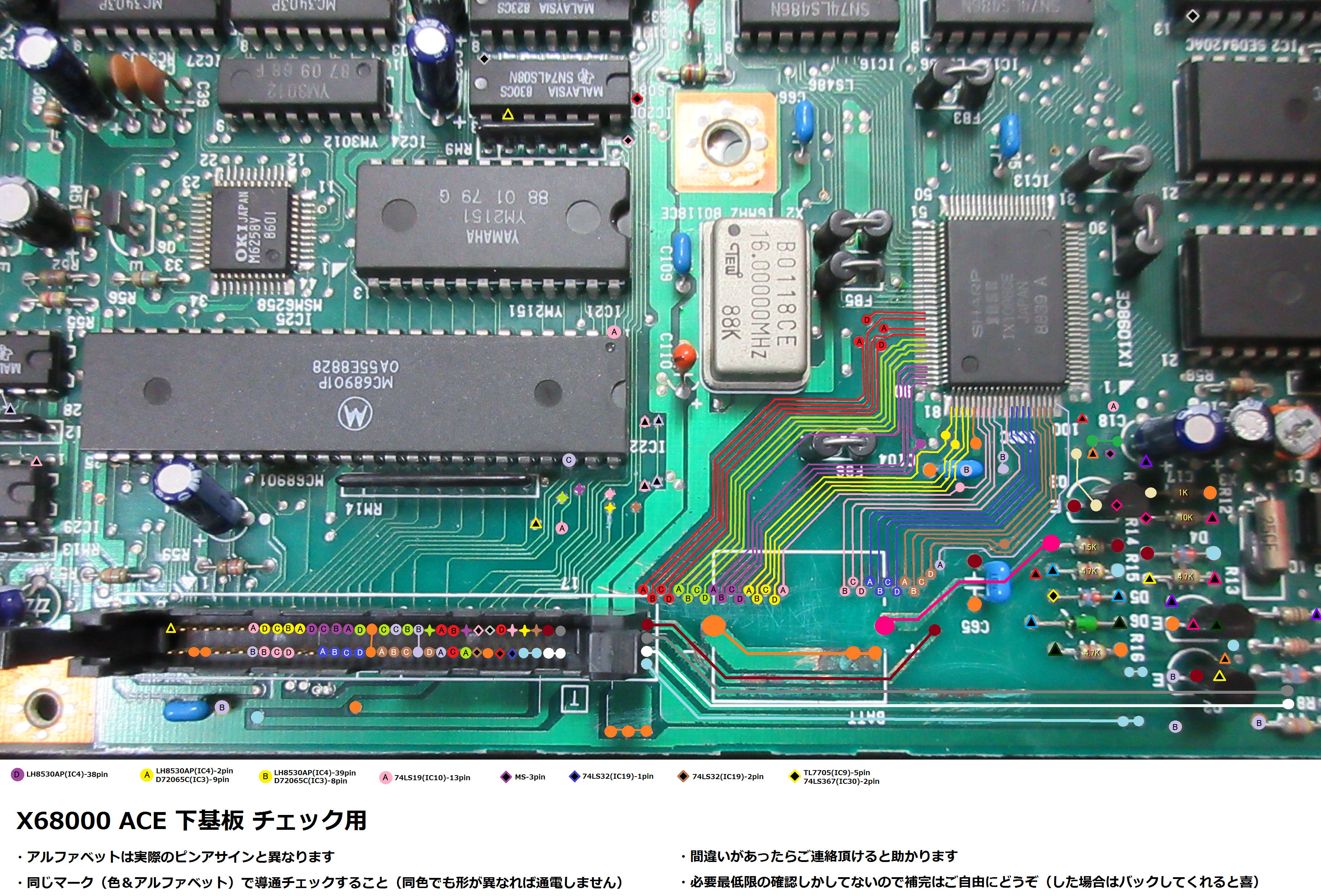
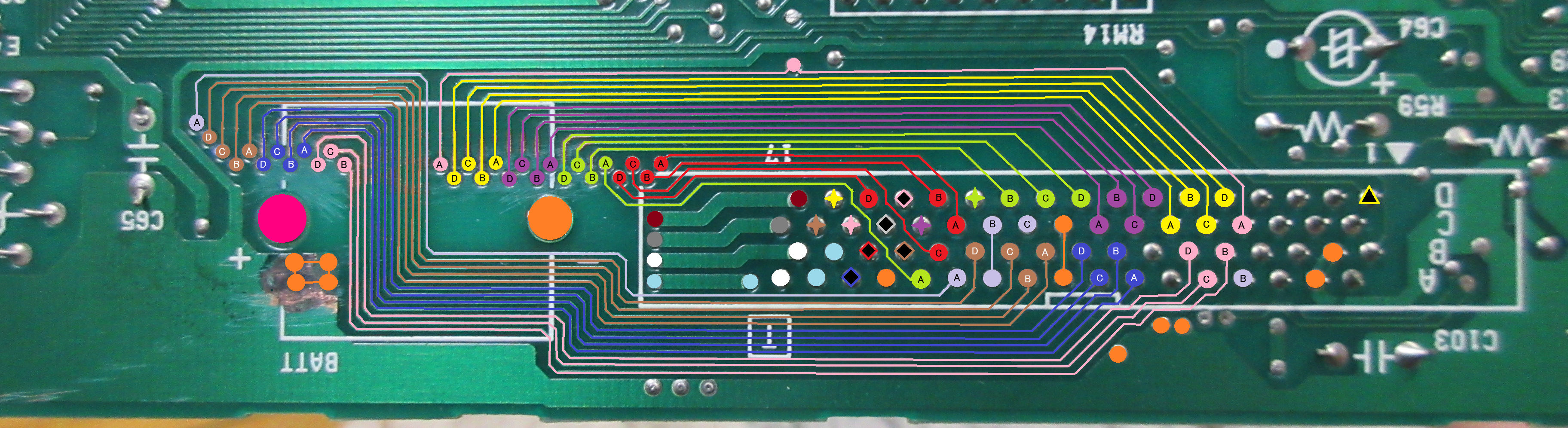
I did a bit more rework on the I/O board and followed some Japanese trace maps I was able to find (thank you Exim; reproduced above) and figured out that the “T” connector seemed continuous with where it was supposed to go. Doing a continuity test on such a high-density connector takes a really long time.
At this point, I was starting to damage traces and pads while reworking things that turned out to be fine, which was extremely discouraging, and I shelved the machine. Thinking on it, I began to suspect the I/O board was compromised in some way I couldn’t tell.
Luckily, another X68000 ACE – a black one, with a nice case – popped up on Yahoo! Auctions. I could just slam the I/O board from that in, and see if it worked! I was able to score it for more money than I paid for the grey ACE, but it was in even worse shape than the thing I had just beat my head against for months.
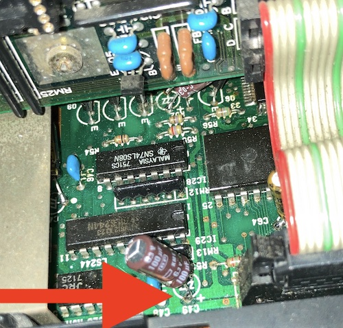
You see, someone has already tried to repair this one. They’ve done a clumsy shotgun recap, and even soldered in a used barrel battery.
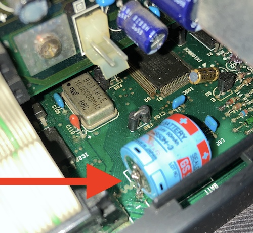
So that’s another project. Just what I needed.
Desperate, I decided that I would depopulate one of the I/O boards, build a reproduction, and swap all the parts across, to rule out any further bad traces and pads and to construct a useful schematic for the ACE. Another good project would be to make a test ROM, which could go in those aforementioned sockets, and do low-level things like check if the TVRAM is okay and if the interrupt table was full of garbage.
However, that’s a BIG PROJECT, and… uh… I didn’t do it. Maybe if I win the lottery, or if the Leaded Solder Patreon replaces my day job.
Inconclusion
Thanks for reading so far! My hope from publishing this article is that someone will come to my rescue and recognize the fault.
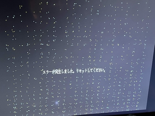
Already, from showing off drafts of this project, it seems like blog friend kak-hoofd has a very similar failure (pictured above.) Although testing out the repair is in early days, so far the cause seems to have been a mechanical failure of a via up near the Messiah chip on the motherboard that only popped up intermittently, so I look forward to a lot of frustrating trace checking and via plugging.
Although this machine has defeated me many times over the last couple of years, I think it is still possible to save. As you can see, it’s come a long way just to give me that error message, and it surely can’t be that much farther to save this grey ACE.
If you have a broken ACE, I hope this at least made you feel better about it. If it helped in any way, let me know!
Repair Summary
| Fault | Remedy | Caveats |
|---|---|---|
| Power supply corroded. | Replace power supply. | |
| Some idiot stripped the hole for the speaker screws. | “Repair” it with super glue. | |
| Extensive battery corrosion has broken traces. | Conduct trace fixes and via stitching on I/O board. | |
| Startup error displayed with corrupt text tiles. | No fix at this time. |
-
I’ve been running EXBIOS on my X68000 PRO for quite some time, with the intent of adding a hard drive, but I haven’t actually finished the power-supply wiring to support that hard drive yet. Be patient! ↩