The Soggy-1000 turns a page
Tags: console sega sg1000 homemade-hardware soggy1000 clone
For version 3 of the Soggy-1000 SG-1000 clone, I wanted to make it more useful as a general-purpose computer. Building a new keyboard is going to cost a fortune in parts, so it’s fiscally prudent to find more reasons to use said keyboard. There are only so many SG-1000 games out there, the SC-3000 software library is kind of small, and I was using only 2k of the 32k of RAM that I had on the board. These are all problems that can be solved with a suitably large application of hubris.
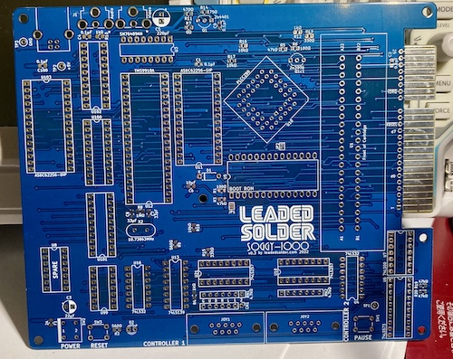
Frequent readers have already seen this version 3 Soggy board, back in the article about testing with the SK-1100 keyboard. Version 3’s not just a pretty new colour, though – there’s lots of bug fixes, cool new features, and general improvements that make it more powerful than a real SG-1000.
The New Stuff
Let’s briefly cover those cool new features, before I start complaining about how much work it was to test and fix them. The version 2 board was perfectly good at playing SG-1000 games, so why bother improving on perfection?
Mostly: because I could. I had so much fun building the SG-1000, and the system is so simple, that it’s easy to think of new features and bug fixes. There’s also a lot of empty memory and I/O map, which provides plenty of places to put those modifications, without having to move too many things around.
There are three major improvements in version three:
- SF-7000 disk drive units can now work (albeit untested;)
- Onboard bootable ROM, used when a cartridge is not inserted;
- 32K of page-switched main memory
We’ll go into each of those three new features in detail below.
SF-7000 Fixes
The images in this section are courtesy of the Joystick Division video on restoring an SF-7000.
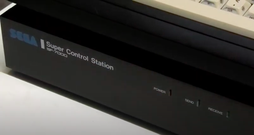
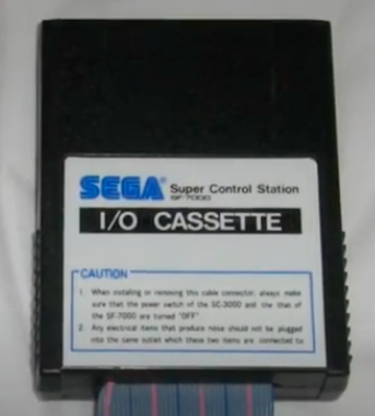
In 1984, facing stiff competition from literally everyone in existence, Sega decided to try and make the SC-3000 more useful by launching the SF-7000 Super Control Station. It features a 3” (yes, 3”) disk drive, serial port, and parallel port, and connects to the computer through the cartridge slot and a very bulky-looking, interference-prone ribbon cable.
Sega does not appear to have sold a lot of these, but the entire thing is completely ridiculous. Reportedly, they had an even crazier one, with an expansion card cage, planned before the whole project died. And people wonder why I love Sega.
Back when I sent the Soggy v2 board off to fabrication, I got to talking to Fabio Della Libera, the individual who helped me with the sound-write-delay problems on the original board, and he mentioned that the SF-7000 disk unit doesn’t work with the original SG-1000. Only the SC-3000 works with it. He’d know, since he made a clone SF-70001!
Since the Soggy is meant to eventually (I hope) be a suitable replacement for an SC-3000, I wanted to make it more like an SC-3000 than like an SG-1000.
I immediately looked into why the SF-7000 unit might not work, and came up with three big theoretical problems by comparing the two systems’ schematics:
- The and (“IO Request + Write,” “IO Request + Read” ) pins were not hooked up on the cartridge slot.
- The SG-1000’s I/O decode for “keyboard” is too greedy, and triggers when the SF-7000’s I/O port range is being accessed. This can write to both devices at once, or cause a bus conflict on read when both of them try to ‘talk’ at the same time.
- The SG-1000 only has 1K of RAM, which may not actually matter… but the SC-3000 has 2K. Better safe than sorry.
To fix the first two problems (more on the RAM later,) I added a 74LS32 OR-gate. It provided a “sub-decode” for the original 74LS139 I/O decoder, such that an access to $e0 –$ff would now decode to nothing instead of . The SF-7000, attached via the cartridge connector, would instead pick this up and do whatever it is that it does with this range2.
I think this will work, but the best way to find out is to build up a protoboard cartridge with a decoder for that address range. Maybe there could be other stuff on that cartridge, too, like a floppy controller?
For now, this “decode defeat” remains untested.
With the remainder of the 74LS32, I synthesized and from “ or ” and “ or ,” respectively. I had used up a total of three gates of the ‘32, which left me with one OR-gate left to implement…
Onboard ROM
The next logical improvement was to add an onboard ROM. After all, the Sega Master System has one, so why shouldn’t this?
On the Master System, the system boots off an onboard BIOS ROM, which later transfers control to the cartridge or card inserted. If you start the console with no game inserted, however, most versions of the Master System have a built-in game or two. For instance, the SMS that I got from a garage sale years ago has Hang On and Safari Hunt.
Besides the obvious fun factor of having a built-in game, this feature actually has a lot of value to people who will be building a Soggy board. Virtually none of my readers live in Japan, and if you don’t live in Japan, you can’t really pop out to the neighbourhood Hard Off and get a ¥400 SG-1000 cartridge with which to test your newly-built Soggy system.
This addition doesn’t sound like a very exciting technical challenge, except that I didn’t know how to “detect” the presence or absence of a cartridge. Most of the cartridge systems I was familiar with – including the SMS – booted first into the onboard ROM, and then checked the ROM inside the cartridge slot for a signature and jumped into the code at a known offset. No signature means that there must not be any cartridge in the slot to respond at that address, so the ROM would then go into a different code path. For instance, the ColecoVision tells you to turn the power off and put a cartridge in, and as mentioned previously, the Sega Master System will start a built-in game or lecture you to put in a cartridge depending on the version of its ROM.
Using this signature-checking technique would work, except SG-1000 carts don’t have a header or a signature to check. Sure, I could heuristically determine whether or not it looks like a cartridge or is just empty bus, by sampling a few regions in the cartridge range of memory and looking for something that isn’t $ff. This appears to be what the Japanese Sega Master System does so it can still play SG-1000 carts, but I haven’t studied it very intently.
In either case, the Z80 boots at $0000 , which, on the SG-1000, is normally occupied by the cartridge. That means I’d need to have some way for the ROM to momentarily “step aside” – maybe even copying a program into RAM and then running it – so that it could read the cartridge at the same location. And adding that signature-checking code would limit what ROMs I could actually run in that slot, which would keep users from easily installing “testing” software.
Instead, I decided to go a different, low-tech, low-software route. I had noticed that on all four of my real SG-1000 cartridges, pins B1 and B2 were connected.
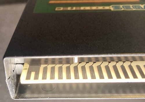
They’re meant to provide the +5V rail, but the traces and fingers are super thick – I can’t imagine what they expected would be attached to the cartridge bus to need so much current. On the SMS and Mark III, the B2 pin becomes a select pin3, so I knew that the cartridge’s guts did not need two separate +5V pins in parallel to give them enough juice to run.
As a result of this research, I could assume the following facts about the system:
- Pins B1 and B2 are always connected on the SG-1000 games;
- Pin B1 is a +5V power supply;
- Therefore, if pin B2 is not connected to +5V on the system side, it will have +5V when a cartridge is inserted
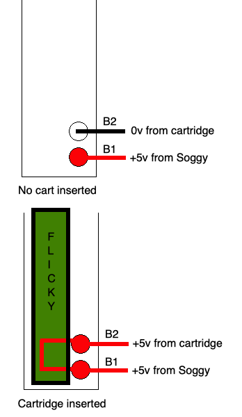
That’s basically an active-high toggle switch! I figured that if I put a weak pull-down on cartridge pin B2 and didn’t otherwise connect it to a power rail, then I could use it to intercept the decode for /EXM2 that would otherwise go to the nonexistent cartridge, and route it to the internal ROM instead.
The aforementioned unused 74LS32 gate from the SF-7000 mods came in handy here, as the select function turns out to be /INT_ROM_SEL = /PIN_B2 or /EXM2. I put all of this behind a jumper, so if any of my assumptions turned out to be wrong, I could just cut the jumper to turn the board back into a normal, ROM-less SG-1000 rather than a piece of waste fibreglass.
I happily implemented this design and then spent several hours re-routing the board to make room for a DIP 27c256. I did consider using a small PLCC one, but it would have been just as much routing work for a bigger pain in the butt to program (adapters! yecch!) and more expensive ROM ICs.
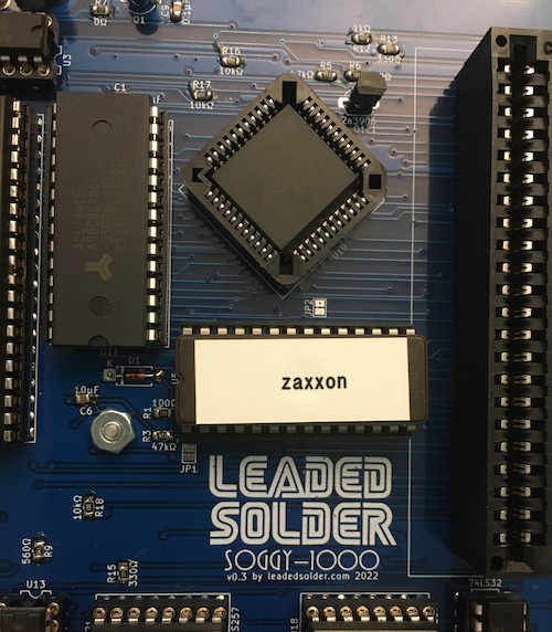
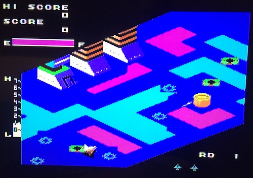
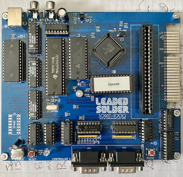
Did it work? Let’s check with this 32kB DIP EPROM marked Zaxxon, which I have socketed into the system. I found this on my workbench, inside my TL866 EPROM writer, for some mysterious reason. I started the system up with no cartridge installed.
Yep, that’s Zaxxon, alright. What if I turn the system off, put in a legitimate retail cartridge like Flicky, and start it up again?
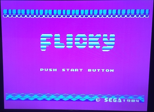
And that’s Flicky. It’s working!
Note that this isn’t exactly an easy way to pirate retail games. Since it only decodes the /EXM2 (i.e. program ROM) signal of the cartridge, any software that relies on /EXM1 for external RAM or a second ROM won’t work as expected. And more games than you’d think did this – Home Mahjong split its software into a 32kByte and 16kByte ROM, several games used two 27c64s, and even Othello added 2kByte of scratch DRAM. BASIC Level IIIB adds a big 3kByte gob of RAM, and even pulls the system’s work-RAM decode line high, so it can take over the entire memory space. Plus, repeatedly swapping DIP EPROMs to change games is no fun, and wears out the socket.
Essentially, this internal ROM slot is the equivalent of the ROM cartridge that I made for the v2 system in the previous entry, just integrated onto the board.
In the future, I have a plan on what to do with this internal ROM slot, one which will maybe even keep me off of Copyright Infringer’s Death Row. It will just take some more time to develop, although its creation will certainly be aided by this other new feature I’m about to talk about…
More RAM
Like on the Leako, I was somewhat forced into using a Cypress 62256 SRAM for main memory on the Soggy. Maybe “forced” is too strong of a word. Nobody makes anything smaller (at least, nothing smaller that’s also cheaper, parallel, and 5V.) That SRAM is relatively big, at 32 kilobytes, and yet the system cannot use most of it – the Leako only addresses 1K, and the earlier Soggys a mere 2K.
All the Soggy boards had (apparently unbeknownst to me in previous articles, thanks to my own bad math) enabled 2K, like an SC-3000 or SG-1000 II, so that more software would work, but what about the remaining thirty kilobytes? Is it doomed to stay forever dim?
No, says the man at Sega. We gave you enough room to map 16k more of it – the range $c000 to $ffff is not decoded by anything else in the system. Which is great – as you know, I’m not good at math, but 16k is like, at least twice as much as 2k. Maybe even four times.
It kept bugging me, though. Solving half the problem is, well, half the problem. Like Solomon, I decided to split that 16k in a way not unlike the Nintendo UNROM mappers, so that the bottom 8k would be fixed, and the top 8k could be switched.
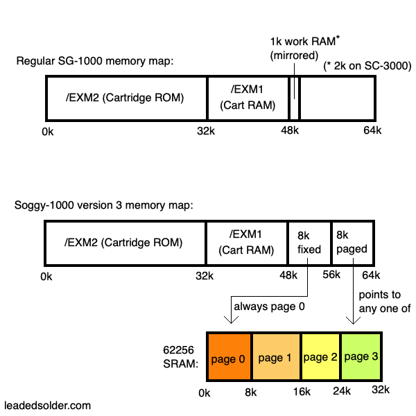
This way, existing SG-1000/SC-3000 programs can pretend that the bottom 2k of RAM is the same as a stock machine. I don’t have to worry about resetting the mapper on system startup or anything. And I can still take advantage of the full 32k by adding a small I/O call to a page-switching port.
I had initially worried that some games relied on mirroring behaviour of the RAM – perhaps counting backwards from $ffff to get some optimization – but the fact that the SC-3000 doubles the RAM to 1k, and there don’t seem to be any compatibility problems, made me feel okay about it. If I run into any broken games, I can always implement a jumper that can be pulled, or hide the memory mapping behind a special I/O port that has to be called to turn it on in the first place.
Great. So how do you actually implement a page-switching scheme?
Writing the Latch
The way I decided to do it was that I would have a latch, which would control the A13 and A14 pins of the 62256. A latch can be thought of as sort of a simple memory: initially I started implementing this with 1-bit flip-flops, and then it became clear that a multi-bit latch would be cheaper.
Specifically, I used an octal latch, a 74LS5734, which true to its name offers eight bits of storage. Since I only have four pages and therefore need only two bits to address them, this meant that six out of the eight “bits” of the latch would remain forever unused, but that’s life.
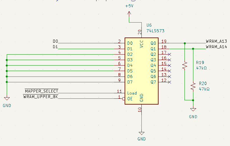
In order to make the latch available to be written to, it needed to be decoded like any other IC. I selected that latch using the existing I/O decoder. Conveniently, there was an extra output free on the 74LS139’s I/O section – thanks, Sega.
To set the memory page that is in use, the programmer would write to the I/O port that addresses the latch. In turn, the 74LS139 decodes that access by looking at the address on the bus, and enables the latch for writing. Then the latch ingests the values of D0 and D1 on the bus, and will “save” them for the next time it’s asked to produce an output. More on that in a bit.
Because of the way it’s been decoded, any I/O write where A7 = 0 and A6 = 0 will select the latch. Although you can write to any address in this range, I will say that the “correct” I/O port to use is $10, because that leaves me some room in the I/O map to add more peripherals later by toggling off of the other address bits. Don’t break forwards compatibility, software developers! You don’t know what crazy thing I could add next!
Setting the latch and reading from the page, then, will work something like this:
out ($10), 2  ; set to page 2 (A13 = 0, A14 = 1)
ld a, ($e000) ; read from the first byte of paged memory (uppermost 8k)
Using the Latch
Because I’ve split the 16k available to me into two 8k windows, I only want to “use” the latch when the programmer is accessing that second, paged, 8k window. As such, I added an extra decode circuit, using a 74LS00 NAND gate.
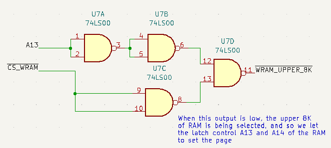
You might think doing this inversion twice is silly. I do too, but I didn’t at the time. I don’t know what I was thinking.
Here’s the truth table. You can also try it yourself in the simulator!
| CPU A13 | /CS_WRAM |
/WRAM_UPPER_8K |
|---|---|---|
| 0 | 0 | 1 |
| 0 | 1 | 1 |
| 1 | 1 | 1 |
| 1 | 0 | 0 (enabled) |
In other words, decoding RAM now goes something like this:
if A13 is high and /CS_WRAM is low:
    enable latch output # sets a13, a14 on ram
    enable ram output # from the existing /CS_WRAM
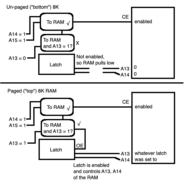
All of this seems pretty confusing if you’re used to programming, like I am, because you have a lot of components all doing their own little job in isolation, instead of a direct chain of procedures responsible for one output.
The most important thing to remember is that the 62256’s A13 and A14 are not the same thing as the CPU’s A13 and A14. On the memory, those are now driven by the latch, and they’re low unless the latch is being used.
This extra little bit of pseudocode might help:
on io decode:
    if io_port >= 0x00 and io_port <= 0x3f:
        set mapper(data_pins)

on memory decode:
    if address >= 48k: # a14 = 1, a15 = 1
        enable 62256 output (a0..a12, a13 = 0, a14 = 0)
        if address >= 56k: # a13 = 1 too
            enable latch output (sets ram a13 and a14)
Or this chart:
I also used the decody program that I wrote for the Leako to write out the memory map. Here it is:
Memory Map:
0000000000000000 /EXM2 (cartridge)
 bits set:
1000000000000000 /EXM1
 bits set: A15
1100000000000000 internal RAM (SG-1000)
 bits set: A14, A15
1110000000000000 second pageable 8K (Soggy-1000 v3+)
 bits set: A13, A14, A15
I/O Map:
0000000000010000 memory mapper (canonical; all $00-3f is available)
 bits set: A4
0000000001000000 psg sn76489
 bits set: A6
0000000010000000 video tms9918
 bits set: A7
0000000011000000 keyboard + joystick
 bits set: A6, A7
0000000011100000 sf-7000
 bits set: A5, A6, A7
One thing that kind of stinks about this design is that there’s no way to ask the latch for what it’s set to. It’s also a little awkward to have to keep track of which page you are working in when you want to make a memory access, but I assume this comes with practice, like driving a stick shift.
Last, a programmer will probably want to make sure their stack pointer is always referencing addresses in the unswitched page window, as I bet weird stuff happens if you switch it away and then do a ret. Same deal if you put your stack at $ffff and then switch away the page containing it5.
Without having written anything to use this model yet, I would assume that you’d want to keep your entire program logic in the ROM or in the first 8K, and decompress resources (or keep massive amounts of game state) in the paged area. This would probably be a good model for a roguelike game, where you have to keep track of what the player has changed on previous floors of the dungeon, or an RPG with a very, very large world map that you can page in and out.
I wasn’t sure if I could change the address pins after the RAM’s output enable had been set. The extra 74LS00 stages would have added some propagation delay (lag) to the setting of those values, not to mention the time for the latch to come online. The datasheet for the 62256 didn’t say I couldn’t do it, but it also didn’t say I could.
Okay, Did It Work?
There’s no point in adding this feature, and then telling everyone on the internet that I added it, without testing it. Nobody tells lies on the internet, especially not about their homebrew Z80 systems.
To cover my bona fides, I quickly added a page-switching test to my reliable RAM-tester ROM that I’ve been adding to in the previous entries. That actual test procedure is nothing spectacular, mostly consisting of writing, changing pages back and forth, and making sure the write ended up on the right page, but it reassured me.
As you can see, it worked flawlessly the first time:
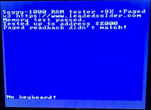
Oh. Uh. Well, that’s embarrassing. My page switching logic seems to not actually work.
Why Didn’t It Work?
I had a primary theory: me being sketchy and changing the address pins on the 62256 SRAM after does not actually work.
Essentially, from a timing perspective, the EPROM sees something like this:
- My pin becomes low and therefore active (directly from })
- My pin becomes low and therefore active at around the same time (directly from the CPU’s )
- Some time later, a signal derived from and sent through a bunch of gates, eventually tells a latch to eventually start driving my high address pins.
When I put it that way, it shouldn’t really be a surprise that it wasn’t working; if I were a ROM-chip designer, I wouldn’t want to have to worry about some nimrod changing the address pins out from under me while I’m still in the process of trying to serve up some sweet, sweet data.
Of course, I had no evidence of this being the problem, not even a scope capture. Rather than get that scope capture, I decided to harass my smart friends about this so-called “timing problem.”
So, I went to ask someone smarter than me how I can solve this timing problem. A lot of smarter people, actually. And then blog friend Chartreuse furrowed his brow, grumbled a little bit, and eventually pointed at the latch itself in my schematic.
The latch’s load pin was marked LOAD. Not . Just LOAD. It was active high, and I was setting it with an active low select off of the 74LS139. D’oh.
Once I realized this, it was a simple bodge to fix it. I cut the trace from between the latch and the ‘139. Then, I stuck a 74LS00 into the “SPARE” DIP socket of the test board6, using it to invert the result of the ‘139, and wired the now active-high LOAD output into the latch.
Did it work?
![With the "load" bodge now working properly, the latch is correctly being written to, and the RAM tester shows that "paging test [has] passed."](/assets/soggy-1k-v0.3-paged-ram-testing-passed.jpg)
Success. I went ahead and changed this in KiCad for version four, and moved on.
Now that we finally know all three of my new features worked, let’s go on and talk about some of the changes and miscellaneous information about this new version-three board.
Layout Changes
Obviously, adding at least four ICs, one of which is a big DIP28 EPROM, is going to take up more room on the board. Despite having a really large board (compared to the teeny Leako, at least) I didn’t quite have enough room to cram everything in.
So, I made it wider. On the original Mark III, the keyboard edge connector is actually flush with the edge of the board, and it has a small recess in the board cut for the sides of the IDC female connector that mates with the male edge connector.
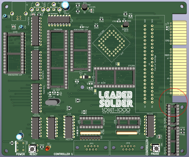
I’m paying JLCPCB for the overall bounding-box of the board, regardless of how much I actually use, so bringing the rest of the board up to flush with the edge connector is free real estate.
This gave me exactly enough room for two more DIPs (the ‘573 latch, and the ‘00 for decode.) Yes, I could have put them on that giant empty space on the left near the video SRAM, but routing the entire data and address bus there would have been very ugly. I’m sure I’ll find something to put there soon enough…
Because I wasn’t able to find technical drawings or datasheets for the keyboard cable’s female IDC head, and the connectors I had ordered were in shipping limbo, I eyeballed some photos on Google Images and decided to leave a 6mm gap on either side of the edge connector. This felt very generous, but it’s better to have a little wasted space than to force a re-spin of the board because of a connector that doesn’t fit.
I also wasn’t too sure about the strain relief when inserting the cartridges, as the machine was still wobbling a little bit on three pins now even further out in space whenever I put the cart in, bending the board. The centre hole that I added on the v0.2 board certainly helps with support, but I need to find some references on “best practices,” because clearly my instincts are no good on this subject. Maybe a case would help stiffen things up, too?
Assembly
As with previous models, assembly was straightforward. Find a pad, put a part in it. Nothing tricky at all, and I even managed to put the Z80 and the VRAM in the right way around the first time.
After blog friend PeteG had some trouble getting colour out of the Soggy with the default 33pF clock capacitors, I put in a pair of 56pF to match the Leako. I’m still not really sure what the right value is, so I think I am going to put in a 33pF and then a series variable-capacitance trimmer cap so I can tweak it. You’ll see more about this a little bit later in the article.
Impossibly, out of all the parts and tools I have lying around in my shop, I had somehow run out of 74LS00 NAND gates, which I assume to be the most common variety of all. This wouldn’t be a problem for the v1 or v2 Soggy boards, but the v3 used 74LS00 to handle the “upper RAM” select for enabling the aforementioned paged-memory mode (and the bodge for fixing it.) Luckily, I had some DIP 74HC00s, and a close perusal of the respective datasheets showed that I’d just barely get away with it.
My first test was with the Home Mahjong cartridge, and the boot EPROM socket unpopulated. It fired right up (once I remembered to turn on the power strip it was connected to.)
Great, a working game. Let’s move on to something trickier. Again, if you’ve read the SK-1100 article, you’re going to be a little spoiled, but try to act surprised. Aunt Myra is getting a bit weird in her old age, but she just wants you to be happy.
Just some BASIC testing
One of the “features” of the SG-1000’s design is that a cartridge can disable the system’s internal work RAM. This is accomplished by pulling up the work RAM’s chip select (a signal we call ) which prevents that chip from being selected.
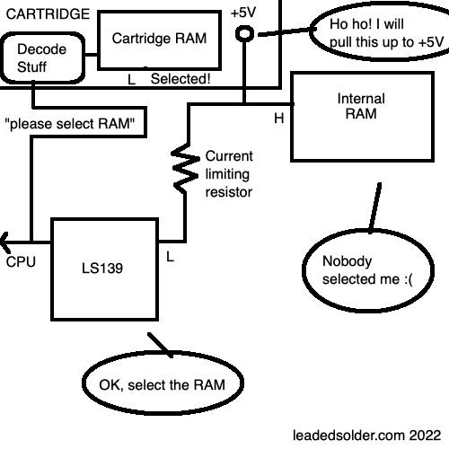
Doing it this way feels dangerous to me, but I don’t think it actually is. The 74LS139 that decodes has a current-limiting resistor in series to that signal, so it shouldn’t blow the output transistor on the chip. And if doing this were a problem, we’d see SG-1000s dropping like flies.
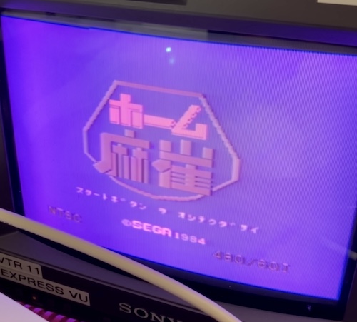
However, I didn’t have any RAM-enabled carts to test this. And my copy of BASIC is only SC-3000 BASIC Level II-A, which doesn’t feature any onboard RAM. The ultimate Sega BASIC cartridge for these machines is Level III-B, which sports 32K of DRAMs on the cartridge. Unfortunately, III-B is incredibly expensive; I remember visiting BEEP in Akihabara and seeing a ¥20k price on it. So I made one instead.
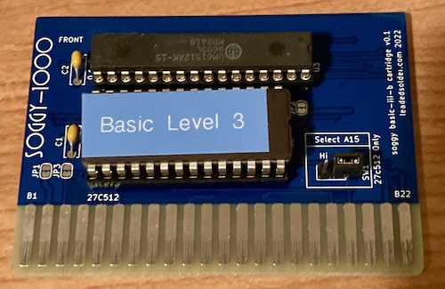
You’ve already seen that cartridge back in the SK-1100 entry, where I used it to test the keyboard. And as you can probably already know, it was great:
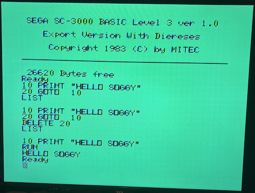
So, a cartridge can take over our RAM, which is another compatibility question solved.
Little Fixes
Not all the problems were related to things I added! I did detect one extra bug that had been lurking since version 2.
Just after I ordered this version 3 board, I started to figure out what would be needed to make an SK-1100 keyboard clone. That’s when I realized that I neglected to run the line to the expansion connector.
On an SC-3000, you poll the joysticks by checking the same 8255 that you would use to look at the keyboard matrix. This is so the arrow keys can do double duty as joystick directional pads, I think. However, on an SG-1000, their buffers are just directly queried using the signal.
As a result, on an SK-1100 keyboard attached to an SG-1000, Sega installed a hack to allow the 8255, when it reaches “row 8” of the matrix, to quickly select the SG-1000’s joystick buffers and make them spew onto the data bus instead, to make it all seem seamless to the software developer.
SMSPower’s expansion port pinout, while otherwise excellent, did not mention this pin’s existence or purpose. I found out I had missed it while going through Enri’s amazing SK-1100 schematic. “Wait, why is here?” I asked. “I don’t have a pin for that…”
Luckily, I was smart enough to leave a through-hole on each tooth of the edge connector. This hole is good for logic probing, but also for bodge wiring! One quick patch wire later, and was now showing up on it.
Sporadic Weirdness
When coming back to my test board after a long period of inactivity, I noticed something weird. I no longer had colour video on the Samsung 910MP monitor, only luminance “colour” bars, and the music in Flicky was all jumbled and screwed up, playing too slow and with the notes ever so slightly out of order. I began to suspect that the crystal feeding the TMS9918, or the TMS9918’s clock divider which controls the CPU and sound chip7, were a little bit drifty. Which is bad, since all of this stuff, except for the VDP and sound chip, are brand new.
Since it was a little cold in the room where I was testing, I ran the board for awhile to see if heating it up would change things. Then, without seeing any results, but still hoping for some kind of miracle, I carried the board into a warmer room, and placed it next to a furnace grate. This, of course, did not work.
It turns out that the Samsung 910MP was set to PAL mode, because (if you’re up on your Leaded Solder lore) I have to tell the TV that it lives in Egypt in order to unlock the SCART port. And, apparently, Egypt is a PAL country8.
When returned to Canada, the television began correctly interpreting the colour output from the NTSC TMS9918. This also explains some of the weird phenomena I’d see from time to time when using the NTSC Genesis with SCART RGB on it.
Jeez, what an embarrassing note on which to end this entry…
Conclusion
Version three of the Soggy-1000 board is a lot better than before. It has a ton of new features which will make it a more useful machine for exploring the wonderful world of software and hardware for the SG/SC series.
Personally, I’m very excited that I was able to add a meaningful “large” feature – page-switching – to an existing computer design. I had felt guilty in the past about hewing my clones too close to the real machines, and wondering if I was actually able to design my own functionality. This has given me a lot of confidence, and now I’m thinking about how to maybe build one of my own computers instead of just copying others.
For the time being… did you notice that mention up above about making changes for Soggy version four?
-
The GitHub repository for the SF-7000 clone has somewhat recently been updated, and involved some excellent collaboration between Fabio and Andrea Ottaviani to debug. I really want to build one! ↩
-
I don’t own an SF-7000, and there sure don’t seem to be many around. Will I make an SF-7000 clone, too? Maybe – it also looks like very common parts, with the exception of the 3” disk drive, and the BIOS ROM appears to be dumped and reverse-engineered. ↩
-
refers to a connector CN4, which appears to be the My Card slot on the Japanese Master System. Any SG-1000 cartridge which shorts +5V to this rail will pull the select up, preventing the card slot from being accessed. This is a cartridge town, little card. You’re a long way from home. ↩
-
The 573 is basically the same thing as the 373, but with a slightly less silly pinout. I may never know why the 373 got the pinout that it did. ↩
-
Just to cover my butt, I wrote a small Bash script to run the z88dk Z80 disassembler on each SG-1000 ROM I had (in a small, but probably complete-ish) collection and grep for stack-pointer writes early on. The only games that put their stack pointer higher than about $c400 seem to be either Taiwanese games (which use the memory expansion pass-through cartridge) or Othello Multivision games (which use the, er, Othello Multivision’s 2K of RAM.) Even those seem to be well within the 8K fixed-page boundary, although many of the Taiwanese games expect RAM to start at $2000 and won’t work without an adapter. I’ll try these out and maybe if any of them are actually good, I’ll build a RAM-stocked cart to play them! ↩
-
Could I have solved this instead by taking out the unnecessary double-invert on the 74LS00 “upper RAM select” and using one of those gates to invert the
LOADsignal? Yes, but those traces were hard to get to in order to sever them, and I was only going to bodge up one board. ↩ -
Update from 2025: I had to take this Soggy board out of storage to do some testing, and the audio glitch reoccurred. Swapping the SN76489 fixed it, so it appears I had a bad sound chip in there the whole time. ↩
-
Wikipedia tells us that Egypt used to be a SECAM country until the early 90s. That must have been an exciting time to be a television salesperson. ↩